background image

 2013 Microchip Technology Inc.

Advance Information

DS33030A-page 165

PIC24FV16KM204 FAMILY

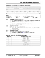
REGISTER 14-3:

SSPxCON1: MSSPx CONTROL REGISTER 1 (SPI MODE)

U-0

U-0

U-0

U-0

U-0

U-0

U-0

U-0

bit 15

bit 8

R/W-0

R/W-0

R/W-0

R/W-0

R/W-0

R/W-0

R/W-0

R/W-0

WCOL

SSPOV

(

1

)

SSPEN

(

2

)

CKP

SSPM3

(

3

)

SSPM2

(

3

)

SSPM1

(

3

)

SSPM0

(

3

)

bit 7

bit 0

Legend:

R = Readable bit

W = Writable bit

U = Unimplemented bit, read as ‘0’

-n = Value at POR

‘1’ = Bit is set

‘0’ = Bit is cleared

x = Bit is unknown

bit 15-8

Unimplemented:

 Read as ‘

0

bit 7

WCOL:

 Write Collision Detect bit

1

 = The SSPxBUF register is written while it is still transmitting the previous word (must be cleared in

software) 

0

 = No collision 

bit 6

SSPOV:

 Master Synchronous Serial Port Receive Overflow Indicator bit

(

1

)

SPI Slave mode: 

1

 = A new byte is received while the SSPxBUF register is still holding the previous data. In case of over-

flow, the data in SSPxSR is lost. Overflow can only occur in Slave mode. The user must read the
SSPxBUF, even if only transmitting data, to avoid setting overflow (must be cleared in software).

0

 = No overflow

bit 5

SSPEN:

 Master Synchronous Serial Port Enable bit

(

2

)


1

 = Enables serial port and configures SCKx, SDOx, SDIx and SSx as serial port pins 

0

 = Disables serial port and configures these pins as I/O port pins

bit 4

CKP:

 Clock Polarity Select bit 

1

 = Idle state for clock is a high level 

0

 = Idle state for clock is a low level

bit 3-0

SSPM<3:0>:

 Master Synchronous Serial Port Mode Select bits

(

3

)

1010

 = SPI Master mode, Clock =


F

OSC

/(2 * ([SSPxADD] + 1))

0101

 = SPI Slave mode, Clock = SCKx pin; SSx pin control is disabled, SSx can be used as an I/O pin 

0100

 = SPI Slave mode, Clock = SCKx pin; SSx pin control is enabled

0011

 = SPI Master mode, Clock = TMR2 output/2 

0010

 = SPI Master mode, Clock = F

OSC

/32 

0001

 = SPI Master mode, Clock = F

OSC

/8 

0000

 = SPI Master mode, Clock = F

OSC

/2

Note 1:

In Master mode, the overflow bit is not set since each new reception (and transmission) is initiated by 
writing to the SSPxBUF register.

2:

When enabled, these pins must be properly configured as inputs or outputs.

3:

Bit combinations not specifically listed here are either reserved or implemented in I

2

C™ mode only. 

Summary of Contents for PIC24FV16KM204 FAMILY

Page 1: ...tage for comparators Band gap reference input Flexible input multiplexing Low power or high speed selection options Charge Time Measurement Unit CTMU Capacitive measurement up to 22 channels Time measurement down to 200 ps resolution Up to 16 external Trigger pairs Internal Temperature Sensor with Dedicated A D Converter Input Multiple Single Capture Compare Peripheral MCCP SCCP Features 16 or 32 ...

Page 2: ... 5 1 3 2 2 2 19 2 2 3 Yes Yes 2 3 FV16KM104 44 16K 1K 512 2 0 5 5 1 1 1 1 1 22 1 Yes 1 3 FV16KM102 28 16K 1K 512 2 0 5 5 1 1 1 1 1 19 1 Yes 1 3 FV08KM102 28 8K 1K 512 2 0 5 5 1 1 1 1 1 19 1 Yes 1 3 FV08KM101 20 8K 1K 512 2 0 5 5 1 1 1 1 1 16 1 Yes 1 3 3V Devices F16KM204 44 16K 2K 512 1 8 3 6 1 3 2 2 2 22 2 2 3 Yes Yes 2 3 F16KM202 28 16K 2K 512 1 8 3 6 1 3 2 2 2 19 2 2 3 Yes Yes 2 3 F08KM204 44 8...

Page 3: ...gging Programmable High Low Voltage Detect HLVD module Programmable Brown out Reset BOR Software enable feature Configurable shutdown in Sleep Auto configures power mode and sensitivity based on device operating speed LPBOR available for re arming of the POR High Performance RISC CPU Modified Harvard Architecture Operating Speed DC 32 MHz clock input 16 MIPS at 32 MHz clock input 8 MHz Internal Os...

Page 4: ...6 PWRLCLK CLCINB CN0 RA4 11 AN19 U1TX CTED1 INT0 CN23 RB7 AN19 U1TX IC1 OC1A CTED1 INT0 CN23 RB7 12 AN20 SCL1 U1CTS OC1B CTED10 CN22 RB8 13 AN21 SDA1 T1CK U1RTS U1BCLK IC2 CLC1O CTED4 CN21 RB9 14 IC1 OC1A INT2 CN8 RA6 VCAP OR VDDCORE 15 AN12 HLVDIN SCK1 OC1C CTED2 CN14 RB12 AN12 HLVDIN SCK1 OC1C CTED2 INT2 CN14 RB12 16 AN11 SDO1 OCFB OC1D CTPLS CN13 RB13 17 CVREF AN10 SDI1 C1OUT OCFA CTED5 INT1 CN...

Page 5: ...RB7 9 AN20 SCL1 U1CTS OC1B CTED10 CN22 RB8 10 AN21 SDA1 T1CK U1RTS U1BCLK IC2 CLC1O CTED4 CN21 RB9 11 IC1 OC1A INT2 CN8 RA6 VCAP OR VDDCORE 12 AN12 HLVDIN SCK1 OC1C CTED2 CN14 RB12 AN12 HLVDIN SCK1 OC1C CTED2 INT2 CN14 RB12 13 AN11 SDO1 OCFB OC1D CTPLS CN13 RB13 14 CVREF AN10 SDI1 C1OUT OCFA CTED5 INT1 CN12 RB14 15 AN9 REFO SS1 TCKIA CTED6 CN11 RB15 16 VSS AVSS 17 VDD AVDD 18 MCLR VPP RA5 MCLR VPP...

Page 6: ...T0 CN23 RB7 17 AN20 SCL1 U1CTS C3OUT OC1B CTED10 CN22 RB8 18 AN21 SDA1 T1CK U1RTS U1BCLK IC2 OC4 CLC1O CTED4 CN21 RB9 19 SDI2 IC1 OC5 CLC2O CTED3 CN9 RA7 20 C2OUT OC1A CTED1 INT2 CN8 RA6 VCAP OR VDDCORE 21 PGD2 SDI1 OC3A OC1C CTED11 CN16 RB10 22 PGC2 SCK1 OC2A CTED9 CN15 RB11 23 DAC1OUT AN12 HLVDIN SS2 IC3 OC2B CTED2 CN14 RB12 DAC1OUT AN12 HLVDIN SS2 IC3 OC2B CTED2 INT2 CN14 RB12 24 OA1INC OA2INC ...

Page 7: ...KI AN13 CN30 RA2 7 OSCO CLKO AN14 CN29 RA3 8 SOSCI AN15 U2RTS U2BCLK CN1 RB4 9 SOSCO SCLKI AN16 PWRLCLK U2CTS CN0 RA4 10 VDD 11 PGD3 AN17 ASDA1 SCK2 IC4 OC1E CLCINA CN27 RB5 12 PGC3 AN18 ASCL1 SDO2 IC5 OC1F CLCINB CN24 RB6 13 AN19 U1TX INT0 CN23 RB7 AN19 U1TX C2OUT OC1A INT0 CN23 RB7 14 AN20 SCL1 U1CTS C3OUT OC1B CTED10 CN22 RB8 15 AN21 SDA1 T1CK U1RTS U1BCLK IC2 OC4 CLC1O CTED4 CN21 RB9 16 SDI2 I...

Page 8: ...EF VREF DAC1REF AN0 C3INC CN2 RA0 CVREF VREF DAC1REF AN0 C3INC CTED1 CN2 RA0 20 CVREF VREF AN1 CN3 RA1 21 PGD1 AN2 CTCMP ULPWU C1IND C2INB C3IND U2TX CN4 RB0 22 PGC1 OA1INA OA2INA AN3 C1INC C2INA U2RX CTED12 CN5 RB1 OA1INA OA2INA AN3 C1INC C2INA U2RX CTED12 CN5 RB1 23 OA1INB OA2INB AN4 C1INB C2IND SDA2 TCKIB CTED13 CN6 RB2 24 OA1OUT AN5 C1INA C2INC SCL2 CN7 RB3 25 AN6 CN32 RC0 26 AN7 CN31 RC1 27 A...

Page 9: ...INA AN3 C1INC C2INA U2RX CTED12 CN5 RB1 25 OA1INB OA2INB AN4 C1INB C2IND SDA2 TCKIB CTED13 CN6 RB2 AN4 C1INB C2IND SDA2 T5CK T4CK CTED13 CN6 RB2 26 OA1OUT AN5 C1INA C2INC SCL2 CN7 RB3 27 AN6 CN32 RC0 28 AN7 CN31 RC1 29 AN8 CN10 RC2 30 VDD 31 VSS 32 n c 33 OSCI AN13 CLKI CN30 RA2 34 OSCO CLKO AN14 CN29 RA3 35 OCFB CN33 RA8 36 SOSCI AN15 U2RTS U2BCLK CN1 RB4 37 SOSCO SCLKI AN16 PWRLCLK U2CTS CN0 RA4...

Page 10: ... 15 0 Universal Asynchronous Receiver Transmitter UART 173 16 0 Real Time Clock and Calendar RTCC 181 17 0 Configurable Logic Cell CLC 195 18 0 High Low Voltage Detect HLVD 207 19 0 12 Bit A D Converter with Threshold Detect 209 20 0 8 Bit Digital to Analog Converter DAC 229 21 0 Dual Operational Amplifier Module 233 22 0 Comparator Module 235 23 0 Comparator Voltage Reference 239 24 0 Charge Time...

Page 11: ...om You can determine the version of a data sheet by examining its literature number found on the bottom outside corner of any page The last character of the literature number is the version number e g DS30000A is version A of document DS30000 Errata An errata sheet describing minor operational differences from the data sheet and recommended workarounds may exist for current devices As device docum...

Page 12: ...PIC24FV16KM204 FAMILY DS33030A page 12 Advance Information 2013 Microchip Technology Inc NOTES ...

Page 13: ... allowing users to incorporate power saving ideas into their software designs Doze Mode Operation when timing sensitive applications such as serial communications require the uninterrupted operation of peripherals the CPU clock speed can be selectively reduced allowing incremental power savings without missing a beat Instruction Based Power Saving Modes to allow the microcontroller to suspend all ...

Page 14: ...nversion to be initiated without waiting for a sampling period and faster sampling speed The 16 deep result buffer can be used either in Sleep to reduce power or in Active mode to improve throughput Charge Time Measurement Unit CTMU Interface The PIC24FV16KM204 family includes the new CTMU interface module which can be used for capacitive touch sensing proximity sensing and also for precision time...

Page 15: ...24 Timers 11 One 16 Bit Timer five MCCP SCCP with up to two 16 32 timers each Capture Compare PWM modules MCCP SCCP 3 2 Serial Communications MSSP UART 2 2 Input Change Notification Interrupt 37 23 12 Bit Analog to Digital Module input channels 22 22 19 19 Analog Comparators 3 8 Bit Digital to Analog Converters 2 Operational Amplifiers 2 Charge Time Measurement Unit CTMU Yes Real Time Clock and Ca...

Page 16: ...ins 38 24 18 Timers 5 One 16 Bit Timer two MCCP SCCP with up to two 16 32 timers each Capture Compare PWM modules MCCP SCCP 1 1 Serial Communications MSSP UART 1 1 Input Change Notification Interrupt 37 23 17 12 Bit Analog to Digital Module input channels 22 19 16 Analog Comparators 1 8 Bit Digital to Analog Converters Operational Amplifiers Charge Time Measurement Unit CTMU Yes Real Time Clock an...

Page 17: ...Pins 37 23 Timers 11 One 16 Bit Timer five MCCP SCCP with up to two 16 32 timers each Capture Compare PWM modules MCCP SCCP 3 2 Serial Communications MSSP UART 2 2 Input Change Notification Interrupt 36 22 12 Bit Analog to Digital Module input channels 22 19 Analog Comparators 3 8 Bit Digital to Analog Converters 2 Operational Amplifiers 2 Charge Time Measurement Unit CTMU Yes Real Time Clock and ...

Page 18: ... I O Pins 37 23 17 Timers 5 One 16 Bit Timer two MCCP SCCP with up to two 16 32 timers each Capture Compare PWM modules MCCP SCCP 1 1 Serial Communications MSSP UART 1 1 Input Change Notification Interrupt 36 22 16 12 Bit Analog to Digital Module input channels 22 19 16 Analog Comparators 1 8 Bit Digital to Analog Converters Operational Amplifiers Charge Time Measurement Unit CTMU Yes Real Time Cl...

Page 19: ...als 16 16 16 x 16 W Reg Array Multiplier 17x17 PORTA 1 RA 0 7 PORTB 1 RB 0 15 Note 1 All pins or features are not implemented on all device pinout configurations See Table 1 5 for I O port pin descriptions Comparators MCCP1 3 CTMU Op Amp A D 12 Bit DAC1 2 MSSP1 2 CLC1 2 CN1 36 1 UART1 2 Data EEPROM OSCI CLKI OSCO CLKO VDD VSS Timing Generation MCLR Power up Timer Oscillator Start up Timer Power on...

Page 20: ...A A D Analog Inputs AN12 15 23 20 10 11 15 23 20 10 11 I ANA A D Analog Inputs AN13 7 9 6 30 33 7 9 6 30 33 I ANA A D Analog Inputs AN14 8 10 7 31 34 8 10 7 31 34 I ANA A D Analog Inputs AN15 9 11 8 33 36 9 11 8 33 36 I ANA A D Analog Inputs AN16 10 12 9 34 37 10 12 9 34 37 I ANA A D Analog Inputs AN17 14 11 41 45 14 11 41 45 I ANA A D Analog Inputs AN18 15 12 42 46 15 12 42 46 I ANA A D Analog In...

Page 21: ...4 O System Clock Output CN0 10 12 9 34 37 10 12 9 34 37 I ST Interrupt on Change Inputs CN1 9 11 8 33 36 9 11 8 33 36 I ST Interrupt on Change Inputs CN2 2 2 27 19 21 2 2 27 19 21 I ST Interrupt on Change Inputs CN3 3 3 28 20 22 3 3 28 20 22 I ST Interrupt on Change Inputs CN4 4 4 1 21 23 4 4 1 21 23 I ST Interrupt on Change Inputs CN5 5 5 2 22 24 5 5 2 22 24 I ST Interrupt on Change Inputs CN6 6 ...

Page 22: ...puts CN26 38 41 38 41 I ST Interrupt on Change Inputs CN27 14 11 41 45 14 11 41 45 I ST Interrupt on Change Inputs CN28 36 39 36 39 I ST Interrupt on Change Inputs CN29 8 10 7 31 34 8 10 7 31 34 I ST Interrupt on Change Inputs CN30 7 9 6 30 33 7 9 6 30 33 I ST Interrupt on Change Inputs CN31 26 28 26 28 I ST Interrupt on Change Inputs CN32 25 27 25 27 I ST Interrupt on Change Inputs CN33 32 35 32 ...

Page 23: ...F 3 3 28 20 22 3 3 28 20 22 I ANA Comparator Voltage Reference Negative Input DAC1OUT 23 20 10 11 23 20 10 11 O ANA DAC1 Output DAC1REF 2 27 19 21 2 27 19 21 I ANA DAC1 Positive Voltage Reference Input DAC2OUT 25 22 14 15 25 22 14 15 O ANA DAC2 Output DAC2REF 26 23 15 16 26 23 15 16 I ANA DAC2 Positive Voltage Reference Input HLVDIN 15 23 20 10 11 15 23 20 10 11 I ANA External High Low Voltage Det...

Page 24: ... Compare D OC1E 14 11 41 45 14 11 41 45 O MCCP1 Output Compare E OC1F 15 12 42 46 15 12 42 46 O MCCP1 Output Compare F OC2A 4 22 19 9 10 4 22 19 9 10 O MCCP2 Output Compare A OC2B 23 20 10 11 23 20 10 11 O MCCP2 Output Compare B OC2C 2 2 2 2 O MCCP2 Output Compare C OC2D 3 3 3 3 O MCCP2 Output Compare D OC2E 4 4 4 4 O MCCP2 Output Compare E OC2F 5 5 5 5 O MCCP2 Output Compare F OC3A 21 18 12 13 21...

Page 25: ...6 18 19 I O ST PORTA Pins RA6 14 20 17 7 7 I O ST PORTA Pins RA7 19 16 6 6 19 16 6 6 I O ST PORTA Pins RA8 32 35 32 35 I O ST PORTA Pins RA9 35 38 35 38 I O ST PORTA Pins RA10 12 13 12 13 I O ST PORTA Pins RA11 13 14 13 14 I O ST PORTA Pins RB0 4 4 1 21 23 4 4 1 21 23 I O ST PORTB Pins RB1 5 5 2 22 24 5 5 2 22 24 I O ST PORTB Pins RB2 6 6 3 23 25 6 6 3 23 25 I O ST PORTB Pins RB3 7 4 24 26 7 4 24 ...

Page 26: ...O 18 26 23 15 16 18 26 23 15 16 O Reference Clock Output RTCC 25 22 14 15 25 22 14 15 O Real Time Clock Calendar Output SCK1 15 22 19 9 10 15 22 19 9 10 I O ST MSSP1 SPI Clock SDI1 17 21 18 8 9 17 21 18 8 9 I ST MSSP1 SPI Data Input SDO1 16 24 21 11 12 16 24 21 11 12 O MSSP1 SPI Data Output SS1 18 26 23 15 16 18 26 23 15 16 I ST MSSP1 SPI Slave Select Input SCK2 14 11 38 41 14 11 38 41 I O ST MSSP...

Page 27: ...7 12 9 34 37 I ST UART2 Clear to Send Input U2RTS 11 8 33 36 11 8 33 36 O UART2 Request to Send Output U2BCLK 13 18 15 1 1 13 18 15 1 1 O UART2 16x Baud Rate Clock Output U2RX 5 2 22 24 5 2 22 24 I ST UART2 Receive U2TX 4 1 21 23 4 1 21 23 O UART2 Transmit ULPWU 4 4 1 21 23 4 4 1 21 23 I ANA Ultra Low Power Wake up Input VCAP 14 20 17 7 7 P Regulator External Filter Capacitor Connection VDD 20 28 ...

Page 28: ...PIC24FV16KM204 FAMILY DS33030A page 28 Advance Information 2013 Microchip Technology Inc NOTES ...

Page 29: ... and debugging purposes see Section 2 5 ICSP Pins OSCI and OSCO pins when an external oscillator source is used see Section 2 6 External Oscillator Pins Additionally the following pins may be required VREF VREF pins are used when external voltage reference for analog modules is implemented The minimum mandatory connections are shown in Figure 2 1 FIGURE 2 1 RECOMMENDED MINIMUM CONNECTIONS Note The...

Page 30: ...it is suggested to use a tank capac itor for integrated circuits including microcontrollers to supply a local power source The value of the tank capacitor should be determined based on the trace resistance that connects the power supply source to the device and the maximum current drawn by the device in the application In other words select the tank capacitor so that it meets the acceptable voltag...

Page 31: ...t of this capacitor should be close to VCAP It is recommended that the trace length not exceed 0 25 inch 6 mm Refer to Section 27 0 Electrical Characteristics for additional information Refer to Section 27 0 Electrical Characteristics for information on VDD and VDDCORE FIGURE 2 3 FREQUENCY vs ESR PERFORMANCE FOR SUGGESTED VCAP Note This section applies only to PIC24FV16KM devices with an on chip v...

Page 32: ...eramic capacitors can vary substantially based on the amount of DC voltage applied to the capacitor This effect can be very signifi cant but is often overlooked or is not always documented A typical DC bias voltage vs capacitance graph for X7R type capacitors is shown in Figure 2 4 FIGURE 2 4 DC BIAS VOLTAGE vs CAPACITANCE CHARACTERISTICS When selecting a ceramic capacitor to be used with the inte...

Page 33: ... the pins and components A suitable solution is to tie the broken guard sections to a mirrored ground layer In all cases the guard trace s must be returned to ground In planning the application s routing and I O assign ments ensure that adjacent port pins and other signals in close proximity to the oscillator are benign i e free of high frequencies short rise and fall times and other similar noise...

Page 34: ...PIC24FV16KM204 FAMILY DS33030A page 34 Advance Information 2013 Microchip Technology Inc NOTES ...

Page 35: ...ter Direct and various Register Indirect modes Each group offers up to seven addressing modes Instructions are associated with predefined addressing modes depending upon their functional requirements For most instructions the core is capable of executing a data or program data memory read a working register data read a data memory write and a pro gram instruction memory read per instruction cycle ...

Page 36: ...isibility Page Address Register RCOUNT Repeat Loop Counter Register CORCON CPU Control Register Instruction Decode and Control PCH 16 Program Counter 16 Bit ALU 23 23 24 23 Data Bus Instruction Reg 16 16 x 16 W Register Array Divide Support ROM Latch 16 EA MUX RAGU WAGU 16 16 8 Interrupt Controller Stack Control Logic Loop Control Logic Data Latch Data RAM Address Latch Control Signals to Various ...

Page 37: ...W0 WREG W1 W2 W3 W4 W5 W6 W7 W8 W9 W10 W11 W12 W13 Frame Pointer Stack Pointer PSVPAG 7 0 Program Space Visibility RA 0 RCOUNT 15 0 Repeat Loop Counter SPLIM Stack Pointer Limit SRL Registers or bits are shadowed for PUSH S and POP S instructions 0 0 Page Address Register 15 0 CPU Control Register CORCON SRH W14 W15 DC IPL 2 1 0 IPL3 PSV PC Divider Working Registers Multiplier Registers 15 0 Value...

Page 38: ...U Interrupt Priority Level is 5 13 100 CPU Interrupt Priority Level is 4 12 011 CPU Interrupt Priority Level is 3 11 010 CPU Interrupt Priority Level is 2 10 001 CPU Interrupt Priority Level is 1 9 000 CPU Interrupt Priority Level is 0 8 bit 4 RA REPEAT Loop Active bit 1 REPEAT loop in progress 0 REPEAT loop not in progress bit 3 N ALU Negative bit 1 Result was negative 0 Result was non negative z...

Page 39: ...ted hardware multiplier and support hardware division for 16 bit divisor 3 3 1 MULTIPLIER The ALU contains a high speed 17 bit x 17 bit multiplier It supports unsigned signed or mixed sign operation in several multiplication modes 16 bit x 16 bit signed 16 bit x 16 bit unsigned 16 bit signed x 5 bit literal unsigned 16 bit unsigned x 16 bit unsigned 16 bit unsigned x 5 bit literal unsigned 16 bit ...

Page 40: ...e per bit of divisor so both 32 bit 16 bit and 16 bit 16 bit instructions take the same number of cycles to execute 3 3 3 MULTI BIT SHIFT SUPPORT The PIC24F ALU supports both single bit and single cycle multi bit arithmetic and logic shifts Multi bit shifts are implemented using a shifter block capable of performing up to a 15 bit arithmetic right shift or up to a 15 bit left shift in a single cyc...

Page 41: ...ception is the use of TBLRD TBLWT operations which use TBLPAG 7 to permit access to the Configuration bits and Device ID sections of the configuration memory space Memory maps for the PIC24FV16KM204 family of devices are displayed in Figure 4 1 FIGURE 4 1 PROGRAM SPACE MEMORY MAP FOR PIC24FV16KM204 FAMILY DEVICES 000000h 0000FEh 000002h 000100h F80010h F80012h FEFFFEh FFFFFFh 000004h 000200h 0001F...

Page 42: ...errupt Vector Tables located from 000004h to 0000FFh and 000104h to 0001FFh These vector tables allow each of the many device interrupt sources to be handled by separate ISRs Section 8 1 Interrupt Vector IVT Table discusses the Interrupt Vector Tables in more detail 4 1 3 DATA EEPROM In the PIC24FV16KM204 family the data EEPROM is mapped to the top of the user program memory space starting at addr...

Page 43: ...ng on the particular device PIC24FV16KM family devices implement either 512 or 1024 words of data memory Should an EA point to a location outside of this area an all zero word or byte will be returned 4 2 1 DATA SPACE WIDTH The data memory space is organized in byte addressable 16 bit wide blocks Data is aligned in data memory and registers as 16 bit words but all the data space EAs resolve to byt...

Page 44: ...ion is provided to allow the users to translate 8 bit signed data to 16 bit signed values Alternatively for 16 bit unsigned data users can clear the MSB of any W register by executing a Zero Extend ZE instruction on the appropriate address Although most instructions are capable of operating on word or byte data sizes it should be noted that some instructions operate only on words 4 2 3 NEAR DATA S...

Page 45: ...0 WREG12 18h WREG12 0000 WREG13 1Ah WREG13 0000 WREG14 1Ch WREG14 0000 WREG15 1Eh WREG15 0800 SPLIM 20h SPLIM xxxx PCL 2Eh PCL 0000 PCH 30h PCH7 PCH6 PCH5 PCH4 PCH3 PCH2 PCH1 PCH0 0000 TBLPAG 32h TBLPAG7 TBLPAG6 TBLPAG5 TBLPAG4 TBLPAG3 TBLPAG2 TBLPAG1 TBLPAG0 0000 PSVPAG 34h PSVPAG7 PSVPAG6 PSVPAG5 PSVPAG4 PSVPAG3 PSVPAG2 PSVPAG1 PSVPAG0 0000 RCOUNT 36h RCOUNT xxxx SR 42h DC IPL2 IPL1 IPL0 RA N OV...

Page 46: ...CN9IE 1 2 CN7IE 1 2 CN6IE CN5IE CN4IE CN3IE CN2IE CN1IE CN0IE 0000 CNEN2 64h CN31IE 2 CN30IE CN29IE CN28IE 2 CN27IE 1 2 CN26IE 2 CN25IE 2 CN24IE 1 2 CN23IE CN22IE CN21IE CN20IE 2 CN19IE 2 CN18IE 2 CN17IE 2 CN16IE 1 2 0000 CNEN3 66h CN36IE 2 CN35IE 2 CN34IE 2 CN33IE 2 CN32IE 2 0000 CNPU1 6Eh CN15PUE 1 2 CN14PUE CN13PUE CN12PUE CN11PUE CN10PUE 2 CN9PUE 1 2 CN7PUE 1 2 CN6PUE CN5PUE CN4PUE CN3PUE CN2P...

Page 47: ...T1IP0 CCP2IP2 CCP2IP1 CCP2IP0 CCP1IP2 CCP1IP1 CCP1IP0 INT0IP2 INT0IP1 INT0IP0 4444 IPC1 A6h CCT1IP2 CCT1IP1 CCT1IP0 CCP4IP2 CCP4IP1 CCP4IP0 CCP3IP2 CCP3IP1 CCP3IP0 4440 IPC2 A8h U1RXIP2 U1RXIP1 U1RXIP0 CCT2IP2 CCT2IP1 CCT2IP0 4004 IPC3 AAh NVMIP2 NVMIP1 NVMIP0 AD1IP2 AD1IP1 AD1IP0 U1TXIP2 U1TXIP1 U1TXIP0 4044 IPC4 ACh CNIP2 CNIP1 CNIP0 CMIP2 CMIP1 CMIP0 BCL1IP2 BCL1IP1 BCL1IP0 SSP1IP2 SSP1IP1 SSP1...

Page 48: ...L G3POL G2POL G1POL 0000 CLC1SEL 126h DS42 DS41 DS40 DS32 DS31 DS30 DS22 DS21 DS20 DS12 DS11 DS10 0000 CLC1GLSL 12Ah G2D4T G2D4N G2D3T G2D3N G2D2T G2D2N G2D1T G2D1N G1D4T G1D4N G1D3T G1D3N G1D2T G1D2N G1D1T G1D1N 0000 CLC1GLSH 12Ch G4D4T G4D4N G4D3T G4D3N G4D2T G4D2N G4D1T G4D1N G3D4T G3D4N G3D3T G3D3N G3D2T G3D2N G3D1T G3D1N 0000 CLC2CONL 1 12Eh LCEN INTP INTN LCOE LCOUT LCPOL MODE2 MODE1 MODE0 0...

Page 49: ... OCBEN OCAEN ICGSM1 ICGSM0 AUXOUT1 AUXOUT0 ICS2 ICS1 ICS0 0100 CCP1CON3L 148h DT5 DT4 DT3 DT2 DT1 DT0 0000 CCP1CON3H 14Ah OETRIG OSCNT2 OSCNT1 OSCNT0 OUTM2 OUTM1 OUTM0 POLACE POLBDF PSSACE1 PSSACE0 PSSBDF1 PSSBDF0 0000 CCP1STATL 14Ch CCPTRIG TRSET TRCLR ASEVT SCEVT ICDIS ICOV ICBNE 0000 CCP1TMRL 150h Time Base Register Low Word 0000 CCP1TMRH 152h Time Base Register High Word 0000 CCP1PRL 154h Time...

Page 50: ...AUXOUT0 ICSEL2 ICSEL1 ICSEL0 0100 CCP2CON3L 16Ch DT5 DT4 DT3 DT2 DT1 DT0 0000 CCP2CON3H 16Eh OETRIG OSCNT2 OSCNT1 OSCNT0 OUTM2 1 OUTM1 1 OUTM0 1 POLACE POLBDF 1 PSSACE1 PSSACE0 PSSBDF1 1 PSSBDF0 1 0000 CCP2STATL 170h CCPTRIG TRSET TRCLR ASEVT SCEVT ICDIS ICOV ICBNE 0000 CCP2TMRL 174h Time Base Register Low Word 0000 CCP2TMRH 176h Time Base Register High Word 0000 CCP2PRL 178h Time Base Period Regi...

Page 51: ...UT0 ICS2 ICS1 ICS0 0100 CCP3CON3L 1 190h DT5 DT4 DT3 DT2 DT1 DT0 0000 CCP3CON3H 1 192h OETRIG OSCNT2 OSCNT1 OSCNT0 OUTM2 OUTM1 OUTM0 POLACE POLBDF PSSACE1 PSSACE0 PSSBDF1 PSSBDF0 0000 CCP3STAT 1 194h CCPTRIG TRSET TRCLR ASEVT SCEVT ICDIS ICOV ICBNE 0000 CCP3TMRL 1 198h Time Base Register Low Word 0000 CCP3TMRH 1 19Ah Time Base Register High Word 0000 CCP3PRL 1 19Ch Time Base Period Register Low Wo...

Page 52: ...GSM1 ICGSM0 AUXOUT1 AUXOUT0 ICSEL2 ICSEL1 ICSEL0 0100 CCP4CON3H 1 1B6h OETRIG OSCNT2 OSCNT1 OSCNT0 POLACE PSSACE1 PSSACE0 0000 CCP4STATL 1 1B8h CCPTRIG TRSET TRCLR ASEVT SCEVT ICDIS ICOV ICBNE 0000 CCP4TMRL 1 1BCh Time Base Register Low Word 0000 CCP4TMRH 1 1BEh Time Base Register High Word 0000 CCP4PRL 1 1C0h Time Base Period Register Low Word FFFF CCP4PRH 1 1C2h Time Base Period Register High Wo...

Page 53: ...CGSM1 ICGSM0 AUXOUT1 AUXOUT0 ICSEL2 ICSEL1 ICSEL0 0100 CCP5CON3H 1 1DAh OETRIG OSCNT2 OSCNT1 OSCNT0 POLACE PSSACE1 PSSACE0 0000 CCP5STATL 1 1DCh CCPTRIG TRSET TRCLR ASEVT SCEVT ICDIS ICOV ICBNE 0000 CCP5TMRL 1 1E0h Time Base Register Low Word 0000 CCP5TMRH 1 1E2h Time Base Register High Word 0000 CCP5PRL 1 1E4h Time Base Period Register Low Word FFFF CCP5PRH 1 1E6h Time Base Period Register High W...

Page 54: ...wn u unchanged unimplemented q value depends on condition r reserved Bold indicates shared access SFRs TABLE 4 14 MSSP2 I2 C SPI REGISTER MAP File Name Addr Bit 15 Bit 14 Bit 13 Bit 12 Bit 11 Bit 10 Bit 9 Bit 8 Bit 7 Bit 6 Bit 5 Bit 4 Bit 3 Bit 2 Bit 1 Bit 0 All Resets SSP2BUF 1 210h MSSP Receive Buffer Transmit Register 00xx SSP2CON1 1 212h WCOL SSPOV SSPEN CKP SSPM3 SSPM2 SSPM1 SSPM0 0000 SSP2CO...

Page 55: ...known u unchanged unimplemented q value depends on condition r reserved Bold indicates shared access SFRs TABLE 4 16 UART2 REGISTER MAP File Name Addr Bit 15 Bit 14 Bit 13 Bit 12 Bit 11 Bit 10 Bit 9 Bit 8 Bit 7 Bit 6 Bit 5 Bit 4 Bit 3 Bit 2 Bit 1 Bit 0 All Resets U2MODE 1 230h UARTEN USIDL IREN RTSMD UEN1 UEN0 WAKE LPBACK ABAUD URXINV BRGH PDSEL1 PDSEL0 STSEL 0000 U2STA 1 232h UTXISEL1 UTXINV UTXI...

Page 56: ...Bit 0 All Resets DAC1CON 1 274h DACEN DACSIDL DACSLP DACFM SRDIS DACTRIG DACOE DACTSEL4 DACTSEL3 DACTSEL2 DACTSEL1 DACTSEL0 DACREF1 DACREF0 0000 DAC1DAT 1 276h DACDAT15 2 DACDAT14 2 DACDAT13 2 DACDAT12 2 DACDAT11 2 DACDAT10 2 DACDAT9 2 DACDAT8 2 DACDAT7 2 DACDAT6 2 DACDAT5 2 DACDAT4 2 DACDAT3 2 DACDAT2 2 DACDAT1 2 DACDAT0 2 0000 Legend x unknown u unchanged unimplemented q value depends on conditi...

Page 57: ...10 TRISB9 TRISB8 TRISB7 TRISB6 TRISB5 TRISB4 TRISB3 TRISB2 TRISB1 TRISB0 FFFF 1 PORTB 2CAh RB15 RB14 RB13 RB12 RB11 RB10 RB9 RB8 RB7 RB6 RB5 RB4 RB3 RB2 RB1 RB0 xxxx LATB 2CCh LATB15 LATB14 LATB13 LATB12 LATB11 LATB10 LATB9 LATB8 LATB7 LATB6 LATB5 LATB4 LATB3 LATB2 LATB1 LATB0 xxxx ODCB 2CEh ODB15 ODB14 ODB13 ODB12 ODB11 ODB10 ODB9 ODB8 ODB7 ODB6 ODB5 ODB4 ODB3 ODB2 ODB1 ODB0 0000 Legend x unknown...

Page 58: ... Bit 14 Bit 13 Bit 12 Bit 11 Bit 10 Bit 9 Bit 8 Bit 7 Bit 6 Bit 5 Bit 4 Bit 3 Bit 2 Bit 1 Bit 0 All Resets PADCFG1 2FCh SDO2DIS 1 SCK2DIS 1 SDO1DIS SCK1DIS 0000 Legend x unknown u unchanged unimplemented q value depends on condition r reserved Bold indicates shared access SFRs Note 1 These bits are not available on the PIC24F V 08KM101 device read as 0 ...

Page 59: ...shold for Channel 16 Threshold for Channel 4 16 in Window Compare xxxx ADC1BUF17 322h A D Data Buffer 17 Threshold for Channel 17 Threshold for Channel 5 17 in Window Compare xxxx ADC1BUF18 324h A D Data Buffer 18 Threshold for Channel 18 Threshold for Channel 6 18 in Window Compare xxxx ADC1BUF19 326h A D Data Buffer 19 Threshold for Channel 19 Threshold for Channel 7 19 in Window Compare xxxx AD...

Page 60: ... ANSB2 ANSB1 ANSB0 F3FF 1 ANSC 4E4h ANSC2 2 3 ANSC1 2 3 ANSC0 2 3 0007 1 Legend x unknown u unchanged unimplemented q value depends on condition r reserved Bold indicates shared access SFRs Note 1 Reset value depends on the device type the PIC24F16KM204 value is shown 2 These bits are not implemented in 20 pin devices 3 These bits are not implemented in 28 pin devices TABLE 4 28 REAL TIME CLOCK AN...

Page 61: ...ON COE CPOL CLPWR CEVT COUT EVPOL1 EVPOL0 CREF1 1 CREF0 CCH1 CCH0 0000 CM3CON 1 638h CON COE CPOL CLPWR CEVT COUT EVPOL1 EVPOL0 CREF1 1 CREF0 CCH1 CCH0 0000 Legend x unknown u unchanged unimplemented q value depends on condition r reserved Bold indicates shared access SFRs Note 1 These registers and bits are available only on PIC24F V 16KM2XX devices TABLE 4 30 BAND GAP BUFFER CONTROL REGISTER MAP...

Page 62: ...Bit 6 Bit 5 Bit 4 Bit 3 Bit 2 Bit 1 Bit 0 All Resets NVMCON 760h WR WREN WRERR PGMONLY ERASE NVMOP5 NVMOP4 NVMOP3 NVMOP2 NVMOP1 NVMOP0 0000 NVMKEY 766h NVMKEY7 NVMKEY6 NVMKEY5 NVMKEY4 NVMKEY3 NVMKEY2 NVMKEY1 NVMKEY0 0000 Legend x unknown u unchanged unimplemented q value depends on condition r reserved Bold indicates shared access SFRs TABLE 4 33 ULTRA LOW POWER WAKE UP REGISTER MAP File Name Addr...

Page 63: ...during operation Using table instructions to access individual bytes or words anywhere in the program space Remapping a portion of the program space into the data space PSV Table instructions allow an application to read or write small areas of the program memory This makes the method ideal for accessing data tables that need to be updated from time to time It also allows access to all bytes of th...

Page 64: ...1 0 xxxx xxxx xxx xxxx xxxx xxxx Note 1 Data EA 15 is always 1 in this case but is not used in calculating the program space address Bit 15 of the address is PSVPAG 0 2 PSVPAG can have only two values 00 to access program memory and FF to access data EEPROM on the PIC24F16KM family 0 Program Counter 23 Bits 1 PSVPAG 8 Bits EA 15 Bits Program Counter 1 Select TBLPAG 8 Bits EA 16 Bits Byte Select 0 ...

Page 65: ...d when it is 0 2 TBLRDH Table Read High In Word mode it maps the entire upper word of a program address P 23 16 to a data address Note that D 15 8 the phantom byte will always be 0 In Byte mode it maps the upper or lower byte of the program word to D 7 0 of the data address as above Note that the data will always be 0 when the upper phantom byte is selected byte select 1 In a similar fashion two t...

Page 66: ... lower 16 bits of the 24 bit program word are used to contain the data The upper 8 bits of any program space locations used as data should be programmed with 1111 1111 or 0000 0000 to force a NOP This prevents possible issues should the area of code ever be accidentally executed For operations that use PSV and are executed outside a REPEAT loop the MOV and MOV D instructions will require one instr...

Page 67: ...erase program memory in blocks of 32 64 and 128 instructions 96 192 and 384 bytes at a time The NVMOP 1 0 NVMCON 1 0 bits decide the erase block size 5 1 Table Instructions and Flash Programming Regardless of the method used Flash memory programming is done with the Table Read and Write instructions These allow direct read and write access to the program memory space from the data memory while the...

Page 68: ...wever will wipe out any previous writes All of the Table Write operations are single word writes two instruction cycles because only the buffers are writ ten A programming cycle is required for programming each row 5 3 Enhanced In Circuit Serial Programming Enhanced ICSP uses an on board bootloader known as the Program Executive PE to manage the pro gramming process Using an SPI data frame format ...

Page 69: ...ny set attempt of the WR bit 0 The program or erase operation completed normally bit 12 PGMONLY Program Only Enable bit 4 bit 11 7 Unimplemented Read as 0 bit 6 ERASE Erase Program Enable bit 1 Perform the erase operation specified by the NVMOP 5 0 bits on the next WR command 0 Perform the program operation specified by the NVMOP 5 0 bits on the next WR command bit 5 0 NVMOP 5 0 Programming Operat...

Page 70: ...ence for NVMKEY must be used to allow any erase or program operation to proceed After the programming command has been executed the user must wait for the programming time until programming is complete The two instructions following the start of the programming sequence should be NOPs as displayed in Example 5 5 EXAMPLE 5 1 ERASING A PROGRAM MEMORY ROW ASSEMBLY LANGUAGE CODE EXAMPLE 5 2 ERASING A ...

Page 71: ...tch 2nd_program_word MOV LOW_WORD_2 W2 MOV HIGH_BYTE_2 W3 TBLWTL W2 W0 Write PM low word into program latch TBLWTH W3 W0 Write PM high byte into program latch 32nd_program_word MOV LOW_WORD_31 W2 MOV HIGH_BYTE_31 W3 TBLWTL W2 W0 Write PM low word into program latch TBLWTH W3 W0 Write PM high byte into program latch C example using MPLAB C30 define NUM_INSTRUCTION_PER_ROW 64 int __attribute__ space...

Page 72: ...ODE DISI 5 Block all interrupts for next 5 instructions MOV 0x55 W0 MOV W0 NVMKEY Write the 55 key MOV 0xAA W1 MOV W1 NVMKEY Write the AA key BSET NVMCON WR Start the erase sequence NOP 2 NOPs required after setting WR NOP BTSC NVMCON 15 Wait for the sequence to be completed BRA 2 C example using MPLAB C30 asm DISI 5 Block all interrupts for next 5 instructions __builtin_write_NVM Perform unlock s...

Page 73: ... the program or erase cycle and the flag bit to indicate if the operation was successfully performed The lower byte of NVMCOM configures the type of NVM operation that will be performed 6 2 NVMKEY Register The NVMKEY is a write only register that is used to prevent accidental writes or erasures of data EEPROM locations To start any programming or erase sequence the following instructions must be e...

Page 74: ...1 Enables an erase or program operation 0 No operation allowed device clears this bit on completion of the write erase operation bit 13 WRERR Flash Error Flag bit 1 A write operation is prematurely terminated any MCLR or WDT Reset during programming operation 0 The write operation completed successfully bit 12 PGMONLY Program Only Enable bit 1 Write operation is executed without erasing target add...

Page 75: ...t MSb of NVMADRU is always 0 since all addresses lie in the user program space FIGURE 6 1 DATA EEPROM ADDRESSING WITH TBLPAG AND NVM ADDRESS REGISTERS 6 4 Data EEPROM Operations The EEPROM block is accessed using Table Read and Write operations similar to those used for program memory The TBLWTH and TBLRDH instructions are not required for data EEPROM operations since the memory is only 16 bits wi...

Page 76: ...ight word erase can be done This example uses C library procedures to manage the Table Pointer builtin_tblpage and builtin_tbloffset and the Erase Page Pointer builtin_tblwtl The memory unlock sequence builtin_write_NVM also sets the WR bit to initiate the operation and returns control when complete EXAMPLE 6 2 SINGLE WORD ERASE int __attribute__ space eedata eeData 0x1234 The variable eeData must...

Page 77: ... the key sequence to NVMKEY Set the WR bit to begin the erase cycle Either poll the WR bit or wait for the NVM interrupt NVMIF is set To get cleared wait until NVMIF is set A typical single word write sequence is provided in Example 6 4 EXAMPLE 6 3 DATA EEPROM BULK ERASE EXAMPLE 6 4 SINGLE WORD WRITE TO DATA EEPROM Set up NVMCON to bulk erase the data EEPROM NVMCON 0x4050 Disable Interrupts For 5 ...

Page 78: ...rdl procedures from the C30 compiler library is provided in Example 6 5 Program Space Visibility PSV can also be used to read locations in the data EEPROM EXAMPLE 6 5 READING THE DATA EEPROM USING THE TBLRD COMMAND int __attribute__ space eedata eeData 0x1234 int data Data read from EEPROM The variable eeData must be a Global variable declared outside of any method the code following this comment ...

Page 79: ... user may set or clear any bit at any time during code execution The RCON bits only serve as status bits Setting a particular Reset status bit in software will not cause a device Reset to occur The RCON register also has other bits associated with the Watchdog Timer WDT and device power saving states The function of these bits is discussed in other sections of this manual FIGURE 7 1 RESET SYSTEM B...

Page 80: ...d voltage supply provided by the Retention Regulator RETREG during Sleep 0 Regulated voltage supply provided by the main Voltage Regulator VREG during Sleep bit 11 10 Unimplemented Read as 0 bit 9 CM Configuration Word Mismatch Reset Flag bit 1 A Configuration Word Mismatch Reset has occurred 0 A Configuration Word Mismatch Reset has not occurred bit 8 PMSLP Program Memory Power During Sleep bit 1...

Page 81: ...rred Flag Bit Setting Event Clearing Event TRAPR RCON 15 Trap Conflict Event POR IOPUWR RCON 14 Illegal Opcode or Uninitialized W Register Access POR CM RCON 9 Configuration Mismatch Reset POR EXTR RCON 7 MCLR Reset POR SWR RCON 6 RESET Instruction POR WDTO RCON 4 WDT Time out PWRSAV Instruction POR SLEEP RCON 3 PWRSAV SLEEP Instruction POR IDLE RCON 2 PWRSAV IDLE Instruction POR BOR RCON 1 POR BO...

Page 82: ...nal is released TABLE 7 3 RESET DELAY TIMES FOR VARIOUS DEVICE RESETS Reset Type Clock Source Determinant POR FNOSCx Configuration bits FNOSC 10 8 BOR MCLR COSCx Control bits OSCCON 14 12 WDTO SWR Reset Type Clock Source SYSRST Delay System Clock Delay Notes POR 6 EC TPOR TPWRT 1 2 FRC FRCDIV TPOR TPWRT TFRC 1 2 3 LPRC TPOR TPWRT TLPRC 1 2 3 ECPLL TPOR TPWRT TLOCK 1 2 4 FRCPLL TPOR TPWRT TFRC TLOC...

Page 83: ...and the programmed values of the FNOSCx bits in the Flash Configuration Word FOSCSEL 2 0 see Table 7 2 The RCFGCAL and NVMCON registers are only affected by a POR 7 4 Brown out Reset BOR The PIC24FV16KM204 family devices implement a BOR circuit which provides the user several configuration and power saving options The BOR is controlled by the BORV 1 0 and BOREN 1 0 Configuration bits FPOR 6 5 1 0 ...

Page 84: ... of BOR alone A more reliable method is to simultaneously check the state of both POR and BOR This assumes that the POR and BOR bits are reset to 0 in the software immediately after any POR event If the BOR bit is 1 while POR is 0 it can be reliably assumed that a BOR event has occurred 7 4 4 DISABLING BOR IN SLEEP MODE When BOREN 1 0 10 BOR remains under hardware control and operates as previousl...

Page 85: ... summarized in Table 8 1 8 1 1 ALTERNATE INTERRUPT VECTOR TABLE AIVT The Alternate Interrupt Vector Table AIVT is located after the IVT as shown in Figure 8 1 Access to the AIVT is provided by the ALTIVT control bit INTCON2 15 If the ALTIVT bit is set all interrupt and exception processes will use the alternate vectors instead of the default vectors The alternate vectors are organized in the same ...

Page 86: ... 52 00007Ch Interrupt Vector 53 00007Eh Interrupt Vector 54 000080h Interrupt Vector 116 0000FCh Interrupt Vector 117 0000FEh Reserved 000100h Reserved 000102h Reserved Oscillator Fail Trap Vector Address Error Trap Vector Stack Error Trap Vector Math Error Trap Vector Reserved Reserved Reserved Interrupt Vector 0 000114h Interrupt Vector 1 Interrupt Vector 52 00017Ch Interrupt Vector 53 00017Eh I...

Page 87: ...000016h 000116h IFS0 1 IEC0 1 IPC0 6 4 MCCP1 Time Base 7 000022h 000122h IFS0 7 IEC0 7 IPC1 14 12 MCCP2 Capture Compare 2 000018h 000118h IFS0 2 IEC0 2 IPC0 10 8 MCCP2 Time Base 8 000024h 000124h IFS0 8 IEC0 8 IPC2 2 0 MCCP3 Capture Compare 5 00001Eh 00011Eh IFS0 5 IEC0 5 IPC1 6 4 MCCP3 Time Base 27 00004Ah 00014Ah IFS1 11 IEC1 11 IPC6 14 12 MSSP1 Bus Collision Interrupt 17 000036h 000136h IFS1 1 ...

Page 88: ... assigned to one of eight priority levels The INTTREG register contains the associated interrupt vector number and the new CPU Interrupt Priority Level which are latched into the Vector Number VECNUM 6 0 and the Interrupt Level ILR 3 0 bit fields in the INTTREG register The new Interrupt Priority Level is the priority of the pending interrupt The interrupt sources are assigned to the IFSx IECx and...

Page 89: ...2 3 111 CPU Interrupt Priority Level is 7 15 user interrupts are disabled 110 CPU Interrupt Priority Level is 6 14 101 CPU Interrupt Priority Level is 5 13 100 CPU Interrupt Priority Level is 4 12 011 CPU Interrupt Priority Level is 3 11 010 CPU Interrupt Priority Level is 2 10 001 CPU Interrupt Priority Level is 1 9 000 CPU Interrupt Priority Level is 0 8 Note 1 See Register 3 1 for the descripti...

Page 90: ...ed bit read as 0 n Value at POR 1 Bit is set 0 Bit is cleared x Bit is unknown bit 15 4 Unimplemented Read as 0 bit 3 IPL3 CPU Interrupt Priority Level Status bit 2 1 CPU Interrupt Priority Level is greater than 7 0 CPU Interrupt Priority Level is 7 or less bit 1 0 Unimplemented Read as 0 Note 1 See Register 3 2 for the description of this bit which is not dedicated to interrupt control functions ...

Page 91: ...nown bit 15 NSTDIS Interrupt Nesting Disable bit 1 Interrupt nesting is disabled 0 Interrupt nesting is enabled bit 14 5 Unimplemented Read as 0 bit 4 MATHERR Arithmetic Error Trap Status bit 1 Overflow trap has occurred 0 Overflow trap has not occurred bit 3 ADDRERR Address Error Trap Status bit 1 Address error trap has occurred 0 Address error trap has not occurred bit 2 STKERR Stack Error Trap ...

Page 92: ...Interrupt Vector Table bit 1 Uses Alternate Interrupt Vector Table AIVT 0 Uses standard default Interrupt Vector Table IVT bit 14 DISI DISI Instruction Status bit 1 DISI instruction is active 0 DISI instruction is not active bit 13 3 Unimplemented Read as 0 bit 2 INT2EP External Interrupt 2 Edge Detect Polarity Select bit 1 Interrupt is on the negative edge 0 Interrupt is on the positive edge bit ...

Page 93: ...Status bit 1 Interrupt request has occurred 0 Interrupt request has not occurred bit 10 9 Unimplemented Read as 0 bit 8 CCT2IF Capture Compare 2 Timer Interrupt Flag Status bit 1 Interrupt request has occurred 0 Interrupt request has not occurred bit 7 CCT1IF Capture Compare 1 Timer Interrupt Flag Status bit 1 Interrupt request has occurred 0 Interrupt request has not occurred bit 6 CCP4IF Capture...

Page 94: ...2 CCT4IF Capture Compare 4 Timer Interrupt Flag Status bit 1 Interrupt request has occurred 0 Interrupt request has not occurred bit 11 CCT3IF Capture Compare 3 Timer Interrupt Flag Status bit 1 Interrupt request has occurred 0 Interrupt request has not occurred bit 10 7 Unimplemented Read as 0 bit 6 CCP5IF Capture Compare 5 Event Interrupt Flag Status bit 1 Interrupt request has occurred 0 Interr...

Page 95: ...IFS3 INTERRUPT FLAG STATUS REGISTER 3 U 0 R W 0 HS U 0 U 0 U 0 U 0 U 0 U 0 RTCIF bit 15 bit 8 U 0 U 0 U 0 U 0 U 0 R W 0 HS R W 0 HS U 0 BCL2IF SSP2IF bit 7 bit 0 Legend HS Hardware Settable bit R Readable bit W Writable bit U Unimplemented bit read as 0 n Value at POR 1 Bit is set 0 Bit is cleared x Bit is unknown bit 15 Unimplemented Read as 0 bit 14 RTCIF Real Time Clock and Calendar Interrupt F...

Page 96: ... Interrupt request has not occurred bit 14 DAC1IF Digital to Analog Converter 1 Interrupt Flag Status bit 1 Interrupt request has occurred 0 Interrupt request has not occurred bit 13 CTMUIF CTMU Interrupt Flag Status bit 1 Interrupt request has occurred 0 Interrupt request has not occurred bit 12 9 Unimplemented Read as 0 bit 8 HLVDIF High Low Voltage Detect Interrupt Flag Status bit 1 Interrupt r...

Page 97: ...it 1 Interrupt request has occurred 0 Interrupt request has not occurred REGISTER 8 11 IFS6 INTERRUPT FLAG STATUS REGISTER 6 U 0 U 0 U 0 U 0 U 0 U 0 U 0 U 0 bit 15 bit 8 U 0 U 0 U 0 U 0 U 0 U 0 R W 0 HS R W 0 HS CLC2IF CLC1IF bit 7 bit 0 Legend HS Hardware Settable bit R Readable bit W Writable bit U Unimplemented bit read as 0 n Value at POR 1 Bit is set 0 Bit is cleared x Bit is unknown bit 15 2...

Page 98: ...bit 1 Interrupt request is enabled 0 Interrupt request is not enabled bit 10 9 Unimplemented Read as 0 bit 8 CCT2IE Capture Compare 2 Timer Interrupt Enable bit 1 Interrupt request is enabled 0 Interrupt request is not enabled bit 7 CCT1IE Capture Compare 1 Timer Interrupt Enable bit 1 Interrupt request is enabled 0 Interrupt request is not enabled bit 6 CCP4IE Capture Compare 4 Event Interrupt En...

Page 99: ...T4IE Capture Compare 4 Timer Interrupt Enable bit 1 Interrupt request is enabled 0 Interrupt request is not enabled bit 11 CCT3IE Capture Compare 3 Timer Interrupt Enable bit 1 Interrupt request is enabled 0 Interrupt request is not enabled bit 10 7 Unimplemented Read as 0 bit 6 CCP5IE Capture Compare 5 Event Interrupt Enable bit 1 Interrupt request is enabled 0 Interrupt request is not enabled bi...

Page 100: ...GISTER 8 15 IEC3 INTERRUPT ENABLE CONTROL REGISTER 3 U 0 R W 0 U 0 U 0 U 0 U 0 U 0 U 0 RTCIE bit 15 bit 8 U 0 U 0 U 0 U 0 U 0 R W 0 R W 0 U 0 BCL2IE SSP2IE bit 7 bit 0 Legend R Readable bit W Writable bit U Unimplemented bit read as 0 n Value at POR 1 Bit is set 0 Bit is cleared x Bit is unknown bit 15 Unimplemented Read as 0 bit 14 RTCIE Real Time Clock and Calendar Interrupt Enable bit 1 Interru...

Page 101: ... 0 Interrupt request is not enabled bit 14 DAC1IE Digital to Analog Converter 1 Interrupt Enable bit 1 Interrupt request is enabled 0 Interrupt request is not enabled bit 13 CTMUIE CTMU Interrupt Enable bit 1 Interrupt request is enabled 0 Interrupt request is not enabled bit 12 9 Unimplemented Read as 0 bit 8 HLVDIE High Low Voltage Detect Interrupt Enable bit 1 Interrupt request is enabled 0 Int...

Page 102: ...t Enable bit 1 Interrupt request is enabled 0 Interrupt request is not enabled REGISTER 8 18 IEC6 INTERRUPT ENABLE CONTROL REGISTER 5 U 0 U 0 U 0 U 0 U 0 U 0 U 0 U 0 bit 15 bit 8 U 0 U 0 U 0 U 0 U 0 U 0 R W 0 R W 0 CLC2IE CLC2IE bit 7 bit 0 Legend R Readable bit W Writable bit U Unimplemented bit read as 0 n Value at POR 1 Bit is set 0 Bit is cleared x Bit is unknown bit 15 2 Unimplemented Read as...

Page 103: ...bits 111 Interrupt is Priority 7 highest priority interrupt 001 Interrupt is Priority 1 000 Interrupt source is disabled bit 11 Unimplemented Read as 0 bit 10 8 CCP2IP 2 0 Capture Compare 2 Event Interrupt Priority bits 111 Interrupt is Priority 7 highest priority interrupt 001 Interrupt is Priority 1 000 Interrupt source is disabled bit 7 Unimplemented Read as 0 bit 6 4 CCP1IP 2 0 Capture Compare...

Page 104: ...implemented Read as 0 bit 14 12 CCT1IP 2 0 Capture Compare 1 Timer Interrupt Priority bits 111 Interrupt is Priority 7 highest priority interrupt 001 Interrupt is Priority 1 000 Interrupt source is disabled bit 11 Unimplemented Read as 0 bit 10 8 CCP4IP 2 0 Capture Compare 4 Event Interrupt Priority bits 111 Interrupt is Priority 7 highest priority interrupt 001 Interrupt is Priority 1 000 Interru...

Page 105: ...itable bit U Unimplemented bit read as 0 n Value at POR 1 Bit is set 0 Bit is cleared x Bit is unknown bit 15 Unimplemented Read as 0 bit 14 12 U1RXIP 2 0 UART1 Receiver Interrupt Priority bits 111 Interrupt is Priority 7 highest priority interrupt 001 Interrupt is Priority 1 000 Interrupt source is disabled bit 11 3 Unimplemented Read as 0 bit 2 0 CCT2IP 2 0 Capture Compare 2 Timer Interrupt Prio...

Page 106: ...x Bit is unknown bit 15 Unimplemented Read as 0 bit 14 12 NVMIP 2 0 NVM Interrupt Priority bits 111 Interrupt is Priority 7 highest priority interrupt 001 Interrupt is Priority 1 000 Interrupt source is disabled bit 11 7 Unimplemented Read as 0 bit 6 4 AD1IP 2 0 A D Conversion Complete Interrupt Priority bits 111 Interrupt is Priority 7 highest priority interrupt 001 Interrupt is Priority 1 000 In...

Page 107: ...rupt Priority bits 111 Interrupt is Priority 7 highest priority interrupt 001 Interrupt is Priority 1 000 Interrupt source is disabled bit 11 Unimplemented Read as 0 bit 10 8 CMIP 2 0 Comparator Interrupt Priority bits 111 Interrupt is Priority 7 highest priority interrupt 001 Interrupt is Priority 1 000 Interrupt source is disabled bit 7 Unimplemented Read as 0 bit 6 4 BCL1IP 2 0 MSSP1 I2C Bus Co...

Page 108: ...ritable bit U Unimplemented bit read as 0 n Value at POR 1 Bit is set 0 Bit is cleared x Bit is unknown bit 15 11 Unimplemented Read as 0 bit 10 8 CCP5IP 2 0 Capture Compare 5 Event Interrupt Priority bits 111 Interrupt is Priority 7 highest priority interrupt 001 Interrupt is Priority 1 000 Interrupt source is disabled bit 7 3 Unimplemented Read as 0 bit 2 0 INT1IP 2 0 External Interrupt 1 Priori...

Page 109: ...8 U 0 U 0 U 0 U 0 U 0 U 0 U 0 U 0 bit 7 bit 0 Legend R Readable bit W Writable bit U Unimplemented bit read as 0 n Value at POR 1 Bit is set 0 Bit is cleared x Bit is unknown bit 15 Unimplemented Read as 0 bit 14 12 CCT3IP 2 0 Capture Compare 3 Timer Interrupt Priority bits 111 Interrupt is Priority 7 highest priority interrupt 001 Interrupt is Priority 1 000 Interrupt source is disabled bit 11 0 ...

Page 110: ...nterrupt Priority bits 111 Interrupt is Priority 7 highest priority interrupt 001 Interrupt is Priority 1 000 Interrupt source is disabled bit 11 Unimplemented Read as 0 bit 10 8 U2RXIP 2 0 UART2 Receiver Interrupt Priority bits 111 Interrupt is Priority 7 highest priority interrupt 001 Interrupt is Priority 1 000 Interrupt source is disabled bit 7 Unimplemented Read as 0 bit 6 4 INT2IP 2 0 Extern...

Page 111: ... 0 U 0 U 0 CCT5IP2 CCT5IP1 CCT5IP0 bit 7 bit 0 Legend R Readable bit W Writable bit U Unimplemented bit read as 0 n Value at POR 1 Bit is set 0 Bit is cleared x Bit is unknown bit 15 7 Unimplemented Read as 0 bit 6 4 CCT5IP 2 0 Capture Compare 5 Timer Interrupt Priority bits 111 Interrupt is Priority 7 highest priority interrupt 001 Interrupt is Priority 1 000 Interrupt source is disabled bit 3 0 ...

Page 112: ...lemented bit read as 0 n Value at POR 1 Bit is set 0 Bit is cleared x Bit is unknown bit 15 11 Unimplemented Read as 0 bit 10 8 BCL2IP 2 0 MSSP2 I2C Bus Collision Interrupt Priority bits 111 Interrupt is Priority 7 highest priority interrupt 001 Interrupt is Priority 1 000 Interrupt source is disabled bit 7 Unimplemented Read as 0 bit 6 4 SSP2IP 2 0 MSSP2 SPI I2C Event Interrupt Priority bits 111 ...

Page 113: ... 0 U 0 U 0 U 0 U 0 U 0 U 0 U 0 bit 7 bit 0 Legend R Readable bit W Writable bit U Unimplemented bit read as 0 n Value at POR 1 Bit is set 0 Bit is cleared x Bit is unknown bit 15 11 Unimplemented Read as 0 bit 10 8 RTCIP 2 0 Real Time Clock and Calendar Interrupt Priority bits 111 Interrupt is Priority 7 highest priority interrupt 001 Interrupt is Priority 1 000 Interrupt source is disabled bit 7 ...

Page 114: ...it U Unimplemented bit read as 0 n Value at POR 1 Bit is set 0 Bit is cleared x Bit is unknown bit 15 11 Unimplemented Read as 0 bit 10 8 U2ERIP 2 0 UART2 Error Interrupt Priority bits 111 Interrupt is Priority 7 highest priority interrupt 001 Interrupt is Priority 1 000 Interrupt source is disabled bit 7 Unimplemented Read as 0 bit 6 4 U1ERIP 2 0 UART1 Error Interrupt Priority bits 111 Interrupt ...

Page 115: ... U 0 U 0 R W 1 R W 0 R W 0 HLVDIP2 HLVDIP1 HLVDIP0 bit 7 bit 0 Legend R Readable bit W Writable bit U Unimplemented bit read as 0 n Value at POR 1 Bit is set 0 Bit is cleared x Bit is unknown bit 15 3 Unimplemented Read as 0 bit 2 0 HLVDIP 2 0 High Low Voltage Detect Interrupt Priority bits 111 Interrupt is Priority 7 highest priority interrupt 001 Interrupt is Priority 1 000 Interrupt source is d...

Page 116: ...plemented Read as 0 bit 14 12 DAC2IP 2 0 Digital to Analog Converter 2 Event Interrupt Priority bits 111 Interrupt is Priority 7 highest priority interrupt 001 Interrupt is Priority 1 000 Interrupt source is disabled bit 11 Unimplemented Read as 0 bit 10 8 DAC1IP 2 0 Digital to Analog Converter 1 Event Interrupt Priority bits 111 Interrupt is Priority 7 highest priority interrupt 001 Interrupt is ...

Page 117: ...s Priority 1 000 Interrupt source is disabled REGISTER 8 34 IPC24 INTERRUPT PRIORITY CONTROL REGISTER 24 U 0 U 0 U 0 U 0 U 0 U 0 U 0 U 0 bit 15 bit 8 U 0 R W 1 R W 0 R W 0 U 0 R W 1 R W 0 R W 0 CLC2IP2 CLC2IP1 CLC2IP0 CLC1IP2 CLC1IP1 CLC1IP0 bit 7 bit 0 Legend R Readable bit W Writable bit U Unimplemented bit read as 0 n Value at POR 1 Bit is set 0 Bit is cleared x Bit is unknown bit 15 7 Unimplem...

Page 118: ...t request is left unacknowledged bit 14 Unimplemented Read as 0 bit 13 VHOLD Vector Hold bit Allows Vector Number Capture and Changes which Interrupt is Stored in the VECNUM 6 0 bits 1 VECNUM 6 0 will contain the value of the highest priority pending interrupt instead of the current interrupt 0 VECNUM 6 0 will contain the value of the last Acknowledged interrupt last interrupt that has occurred wi...

Page 119: ... application In general the user must clear the interrupt flag in the appropriate IFSx register for the source of the interrupt that the ISR handles Otherwise the ISR will be re entered immediately after exiting the routine If the ISR is coded in assembly language it must be termi nated using a RETFIE instruction to unstack the saved PC value SRL value and old CPU priority level 8 4 3 TRAP SERVICE...

Page 120: ...PIC24FV16KM204 FAMILY DS33030A page 120 Advance Information 2013 Microchip Technology Inc NOTES ...

Page 121: ...ency range A Fail Safe Clock Monitor FSCM that detects clock failure and permits safe application recovery or shutdown A simplified diagram of the oscillator system is shown in Figure 9 1 FIGURE 9 1 PIC24FV16KM204 FAMILY CLOCK DIAGRAM Note This data sheet summarizes the features of this group of PIC24F devices It is not intended to be a comprehensive refer ence source For more information on oscil...

Page 122: ...its The Primary Oscillator Configuration bits POSCMD 1 0 FOSC 1 0 and the Initial Oscillator Select Configuration bits FNOSC 2 0 FOSCSEL 2 0 select the oscillator source that is used at a POR The FRC Primary Oscillator with Postscaler FRCDIV is the default unprogrammed selection The secondary oscillator or one of the internal oscillators may be chosen by programming these bit locations The EC mode...

Page 123: ...it R Readable bit W Writable bit U Unimplemented bit read as 0 n Value at POR 1 Bit is set 0 Bit is cleared x Bit is unknown bit 15 Unimplemented Read as 0 bit 14 12 COSC 2 0 Current Oscillator Selection bits 111 8 MHz Fast RC Oscillator with Postscaler FRCDIV 110 500 kHz Low Power Fast RC Oscillator FRC with Postscaler LPFRCDIV 101 Low Power RC Oscillator LPRC 100 Secondary Oscillator SOSC 011 Pr...

Page 124: ...M has detected a clock failure 0 No clock failure has been detected bit 2 SOSCDRV Secondary Oscillator Drive Strength bit 3 1 High power SOSC circuit is selected 0 Low high power select is done via the SOSCSRC Configuration bit bit 1 SOSCEN 32 kHz Secondary Oscillator SOSC Enable bit 1 Enables the secondary oscillator 0 Disables the secondary oscillator bit 0 OSWEN Oscillator Switch Enable bit 1 I...

Page 125: ... 111 1 128 110 1 64 101 1 32 100 1 16 011 1 8 010 1 4 001 1 2 000 1 1 bit 11 DOZEN Doze Enable bit 1 1 DOZE 2 0 bits specify the CPU and peripheral clock ratio 0 CPU and peripheral clock ratio are set to 1 1 bit 10 8 RCDIV 2 0 FRC Postscaler Select bits When COSC 2 0 OSCCON 14 12 111 111 31 25 kHz divide by 256 110 125 kHz divide by 64 101 250 kHz divide by 32 100 500 kHz divide by 16 011 1 MHz di...

Page 126: ...t W Writable bit U Unimplemented bit read as 0 n Value at POR 1 Bit is set 0 Bit is cleared x Bit is unknown bit 15 6 Unimplemented Read as 0 bit 5 0 TUN 5 0 FRC Oscillator Tuning bits 1 011111 Maximum frequency deviation 011110 000001 000000 Center frequency oscillator is running at factory calibrated frequency 111111 100001 100000 Minimum frequency deviation Note 1 Increments or decrements of TU...

Page 127: ...pleted the system clock hardware responds automatically as follows 1 The clock switching hardware compares the COSCx bits with the new value of the NOSCx bits If they are the same then the clock switch is a redundant operation In this case the OSWEN bit is cleared automatically and the clock switch is aborted 2 If a valid clock switch has been initiated the LOCK OSCCON 5 and CF OSCCON 3 bits are c...

Page 128: ...nd allows the user to select a greater range of clock submultiples to drive external devices in the application This reference clock output is controlled by the REFOCON register Register 9 4 Setting the ROEN bit REFOCON 15 makes the clock signal available on the REFO pin The RODIVx bits REFOCON 11 8 enable the selection of 16 different clock divider options The ROSSLP and ROSEL bits REFOCON 13 12 ...

Page 129: ...ce Oscillator Source Select bit 1 Primary oscillator is used as the base clock 1 0 System clock is used as the base clock base clock reflects any clock switching of the device bit 11 8 RODIV 3 0 Reference Oscillator Divisor Select bits 1111 Base clock value divided by 32 768 1110 Base clock value divided by 16 384 1101 Base clock value divided by 8 192 1100 Base clock value divided by 4 096 1011 B...

Page 130: ...PIC24FV16KM204 FAMILY DS33030A page 130 Advance Information 2013 Microchip Technology Inc NOTES ...

Page 131: ...pt WDT time out or a device Reset When the device exits these modes it is said to wake up 10 2 1 SLEEP MODE Sleep mode includes these features The system clock source is shut down If an on chip oscillator is used it is turned off The device current consumption will be reduced to a minimum provided that no I O pin is sourcing current The I O pin directions and states are frozen The Fail Safe Clock ...

Page 132: ...harging the capacitor by configuring RB0 as an input 3 Discharge the capacitor by setting the ULPEN and ULPSINK bits in the ULPWCON register 4 Configure Sleep mode 5 Enter Sleep mode When the voltage on RB0 drops below VIL the device wakes up and executes the next instruction This feature provides a low power technique for periodically waking up the device from Sleep mode The time out is dependent...

Page 133: ...nted bit read as 0 n Value at POR 1 Bit is set 0 Bit is cleared x Bit is unknown bit 15 ULPEN ULPWU Module Enable bit 1 Module is enabled 0 Module is disabled bit 14 Unimplemented Read as 0 bit 13 ULPSIDL ULPWU Stop in Idle Select bit 1 Discontinues module operation when the device enters Idle mode 0 Continues module operation in Idle mode bit 12 9 Unimplemented Read as 0 bit 8 ULPSINK ULPWU Curre...

Page 134: ... the voltage output range of the RETREG This regulator is only used in Sleep mode and has limited output current to maintain the RAM and provide power for limited peripherals such as the WDT while the device is in Sleep It is controlled by the RETCFG Con figuration bit FPOR 2 and in firmware by the RETEN bit RCON 12 RETCFG must be programmed 0 and the RETEN bit must be set 1 for the Retention Regu...

Page 135: ... Control Idle and Doze modes allow users to substantially reduce power consumption by slowing or stopping the CPU clock Even so peripheral modules still remain clocked and thus consume power There may be cases where the application needs what these modes do not provide the allocation of power resources to CPU processing with minimal power consumption from the peripherals PIC24F devices address thi...

Page 136: ...PIC24FV16KM204 FAMILY DS33030A page 136 Advance Information 2013 Microchip Technology Inc NOTES ...

Page 137: ...r operation as digital I O The Data Direction register TRISx determines whether the pin is an input or an output If the data direction bit is a 1 then the pin is an input All port pins are defined as inputs after a Reset Reads from the Data Latch register LAT read the latch Writes to the latch write the latch Reads from the port PORT read the port pins writes to the port pins write the latch Any b...

Page 138: ...t buffer to consume current that exceeds the device specifications 11 2 1 ANALOG SELECTION REGISTER I O pins with shared analog functionality such as A D inputs and comparator inputs must have their digital inputs shut off when analog functionality is used Note that analog functionality includes an analog voltage being applied to the pin externally To allow for analog control the ANSx registers ar...

Page 139: ...ve bit 11 10 Unimplemented Read as 0 bit 9 0 ANSB 9 0 Analog Select Control bits 1 1 Digital input buffer is not active use for analog input 0 Digital input buffer is active Note 1 The ANSB 6 5 3 bits are not available on 20 pin devices REGISTER 11 3 ANSC ANALOG SELECTION PORTC U 0 U 0 U 0 U 0 U 0 U 0 U 0 U 0 bit 15 bit 8 U 0 U 0 U 0 U 0 U 0 R W 1 R W 1 R W 1 ANSC2 1 2 ANSC1 1 2 ANSC0 1 2 bit 7 bi...

Page 140: ...tton or keypad devices are connected On any pin only the pull up resistor or the pull down resistor should be enabled but not both of them If the push button or the keypad is connected to VDD enable the pull down or if they are connected to VSS enable the pull up resistors The pull ups are enabled separately using the CNPU1 and CNPU3 registers which contain the control bits for each of the CNx pin...

Page 141: ...n 1 Set the TON bit 1 2 Select the timer prescaler ratio using the TCKPS 1 0 bits 3 Set the Clock and Gating modes using the TCS and TGATE bits 4 Set or clear the TSYNC bit to configure synchronous or asynchronous operation 5 Load the timer period value into the PR1 register 6 If interrupts are required set the Timer1 Interrupt Enable bit T1IE Use the Timer1 Interrupt Priority bits T1IP 2 0 to set...

Page 142: ...ECS 1 0 Timer1 Extended Clock Select bits 1 11 Reserved do not use 10 Timer1 uses the LPRC as the clock source 01 Timer1 uses the external clock from T1CK 00 Timer1 uses the Secondary Oscillator SOSC as the clock source bit 7 Unimplemented Read as 0 bit 6 TGATE Timer1 Gated Time Accumulation Enable bit When TCS 1 This bit is ignored When TCS 0 1 Gated time accumulation is enabled 0 Gated time accu...

Page 143: ...e a time base gener ator and a common Timer register pair CCPxTMRH L other shared hardware components are added as a particular mode requires Each module has a total of seven control and status registers CCPxCON1L Register 13 1 CCPxCON1H Register 13 2 CCPxCON2L Register 13 3 CCPxCON2H Register 13 4 CCPxCON3L Register 13 5 CCPxCON3H Register 13 6 CCPxSTATL Register 13 7 Each module also includes ei...

Page 144: ...ync Trigger signal like the primary time base The 32 Bit Timer mode uses the CCPxTMRL and CCPxTMRH registers together as a single 32 bit timer When CCPxTMRL overflows CCPxTMRH increments by one This mode provides a simple timer function when it is important to track long time periods Note that the T32 bit CCPxCON1L 5 should be set before the CCPxTMRL or CCPxPRH registers are written to initialize ...

Page 145: ...E 13 4 32 BIT TIMER MODE Comparator CCPxTMRL CCPxPRL CCPxRB CCPxTMRH CCPxPRH Comparator OC Clock Sources Set CCTxIF Special Event Trigger Set CCPxIF SYNC 4 0 Time Base Generator Sync Trigger Control Comparator CCPxTMRL CCPxPRL Comparator Set CCTxIF CCPxTMRH CCPxPRH OC Clock Sources Sync Trigger Control SYNC 4 0 Time Base Generator ...

Page 146: ...001 0 Output High on Compare 16 bit Single Edge Mode 0001 1 Output High on Compare 32 bit 0010 0 Output Low on Compare 16 bit 0010 1 Output Low on Compare 32 bit 0011 0 Output Toggle on Compare 16 bit 0011 1 Output Toggle on Compare 32 bit 0100 0 Dual Edge Compare 16 bit Dual Edge Mode 0101 0 Dual Edge Compare 16 bit buffered PWM Mode 0110 0 Center Aligned Pulse 16 bit buffered Center PWM 0111 0 V...

Page 147: ...xCON1L 4 must be set The T32 and the MOD 3 0 bits are used to select the proper Capture mode as shown in Table 13 3 FIGURE 13 6 INPUT CAPTURE x BLOCK DIAGRAM TABLE 13 3 INPUT CAPTURE MODES MOD 3 0 CCP1CONL 3 0 T32 CCP1CONL 5 Operating Mode 0000 0 Edge Detect 16 bit capture 0000 1 Edge Detect 32 bit capture 0001 0 Every Rising 16 bit capture 0001 1 Every Rising 32 bit capture 0010 0 Every Falling 1...

Page 148: ... 0 control bits CCPxCON2H 4 3 The type of output signal is also dependent on the module operating mode On the PIC24FV16KM204 family of parts the following modules have access to the auxiliary output signal CTMU TABLE 13 4 AUXILIARY OUTPUT AUXOUT 1 0 CCSEL MOD 3 0 Comments Signal Description 00 x xxxx Auxiliary output disabled No Output 01 0 0000 Time Base modes Time Base Period Reset or Rollover 1...

Page 149: ...e bit 1 Module continues to operate in Sleep modes 0 Module does not operate in Sleep modes bit 11 TMRSYNC Time Base Clock Synchronization bit 1 Module time base clock is synchronized to the internal system clocks timing restrictions apply 0 Module time base clock is not synchronized to the internal system clocks bit 10 8 CLKSEL 2 0 CCPx Time Base Clock Select bits 111 External TCLKIA input 110 Ex...

Page 150: ...L 0 Output Compare Timer modes 1111 External Input mode pulse generator is disabled source is selected by ICS 2 0 1110 Reserved 110x Reserved 10xx Reserved 0111 Variable Frequency Pulse mode 0110 Center Aligned Pulse Compare mode buffered 0101 Dual Edge Compare mode buffered 0100 Dual Edge Compare mode 0011 16 Bit 32 Bit Single Edge mode toggle output on compare match 0010 16 Bit 32 Bit Single Edg...

Page 151: ...eriod match 0100 Interrupt every 5th time base period match 0011 Interrupt every 4th time base period match or 4th input capture event 0010 Interrupt every 3rd time base period match or 3rd input capture event 0001 Interrupt every 2nd time base period match or 2nd input capture event 0000 Interrupt after each time base period match or input capture event bit 7 TRIGEN CCPx Trigger Enable bit 1 Trig...

Page 152: ...CCP2 Sync Output 00011 MCCP3 or SCCP3 Sync Output 00100 MCCP4 or SCCP4 Sync Output 00101 MCCP5 or SCCP5 Sync Output 0011x Unused 01000 External Interrupt 0 01001 External Interrupt 1 01010 External Interrupt 2 01011 Timer1 Sync Output 01100 to 10000 Unused 10001 CLC1 Output 10010 CLC2 Output 10011 to 10111 Unused 11000 Comparator 1 11001 Comparator 1 11010 Comparator 1 11011 A D 11100 CTMU 11101 a...

Page 153: ...must be cleared in software to resume PWM activity on output pins bit 14 ASDGM CCPx Auto Shutdown Gate Mode Enable bit 1 Wait until the next Time Base Reset or rollover for shutdown to occur 0 Shutdown event occurs immediately bit 13 Unimplemented Read as 0 bit 12 SSDG CCPx Software Shutdown Gate Control bit 1 Manually force auto shutdown timer clock gate or input capture signal gate event setting...

Page 154: ...ontrolled by the CCPx module the pin is available to the port logic or another peripheral multiplexed on the pin bit 7 6 ICGSM 1 0 Input Capture Gating Source Mode Control bits 11 Reserved 10 One Shot mode falling edge from gating source disables future capture events ICDIS 1 01 One Shot mode rising edge from gating source enables future capture events ICDIS 0 00 Level Sensitive mode a high level ...

Page 155: ... at POR 1 Bit is set 0 Bit is cleared x Bit is unknown bit 15 6 Unimplemented Read as 0 bit 5 0 DT 5 0 Capture Compare PWMx Dead Time Select bits 111111 Insert 63 dead time delay periods between complementary output signals 111110 Insert 62 dead time delay periods between complementary output signals 000010 Insert 2 dead time delay periods between complementary output signals 000001 Insert 1 dead ...

Page 156: ...e base periods 3 time base periods total 001 Extend one shot event by 1 time base period 2 time base periods total 000 Do not extend one shot Trigger event bit 11 Unimplemented Read as 0 bit 10 8 OUTM 2 0 PWMx Output Mode Control bits 1 111 Reserved 110 Output Scan mode 101 Brush DC Output mode forward 100 Brush DC Output mode reverse 011 Reserved 010 Half Bridge Output mode 001 Push Pull Output m...

Page 157: ...location always reads as 0 bit 5 TRCLR CCPx Trigger Clear Request bit Write 1 to this location to cancel the timer Trigger when TRIGEN 1 location always reads as 0 bit 4 ASEVT CCPx Auto Shutdown Event Status Control bit 1 A shutdown event is in progress CCPx outputs are in the shutdown state 0 CCPx outputs operate normally bit 3 SCEVT Single Edge Compare Event Status bit 1 A single edge compare ev...

Page 158: ...PIC24FV16KM204 FAMILY DS33030A page 158 Advance Information 2013 Microchip Technology Inc NOTES ...

Page 159: ... NACKing Selectable Address and Data Hold and Interrupt Masking 14 1 I O Pin Configuration for SPI In SPI Master mode the MSSP module will assert con trol over any pins associated with the SDOx and SCKx outputs This does not automatically disable other digi tal functions associated with the pin and may result in the module driving the digital I O port inputs To prevent this the MSSP module outputs...

Page 160: ...k Select TMR2 Output TOSC Prescaler 4 16 64 2 Edge Select 2 4 Data to TXx RXx in SSPxSR TRIS bit 2 SMP CKE SDOx SDIx SSx SCKx Note Refer to the device data sheet for pin multiplexing Baud Rate Generator SSPxADD 7 0 7 SSPxBUF SSPxSR Serial Input Buffer SSPxBUF Shift Register SSPxSR MSb LSb SDOx SDIx PROCESSOR 1 SCKx SPI Master SSPM 3 0 00xx Serial Input Buffer SSPxBUF Shift Register SSPxSR LSb MSb ...

Page 161: ...for a full list of multiplexed functions SCLx SDAx Start and Stop bit Detect Read Write SSPxBUF SSPxSR Address Mask Start bit Stop bit Internal Data Bus Set Reset S P SSPxSTAT WCOL Shift Clock MSb LSb SDAx Acknowledge Generate Stop bit Detect Write Collision Detect Clock Arbitration State Counter for End of XMIT RCV SCLx SCLx In Bus Collision SDAx In RCV Enable Clock Cntl Clock Arbitrate WCOL Dete...

Page 162: ...t the middle of data output time SPI Slave mode SMP must be cleared when SPI is used in Slave mode bit 6 CKE SPI Clock Select bit 1 1 Transmit occurs on transition from active to Idle clock state 0 Transmit occurs on transition from Idle to active clock state bit 5 D A Data Address bit Used in I2C mode only bit 4 P Stop bit Used in I2C mode only This bit is cleared when the MSSPx module is disable...

Page 163: ...ed In Slave mode 1 Indicates that the last byte received or transmitted was data 0 Indicates that the last byte received or transmitted was address bit 4 P Stop bit 1 1 Indicates that a Stop bit has been detected last 0 Stop bit was not detected last bit 3 S Start bit 1 1 Indicates that a Start bit has been detected last 0 Start bit was not detected last bit 2 R W Read Write Information bit In Sla...

Page 164: ...ude the ACK and Stop bits 0 SSPxBUF is empty does not include the ACK and Stop bits REGISTER 14 2 SSPxSTAT MSSPx STATUS REGISTER I2C MODE CONTINUED Note 1 This bit is cleared on Reset and when SSPEN is cleared 2 This bit holds the R W bit information following the last address match This bit is only valid from the address match to the next Start bit Stop bit or not ACK bit 3 ORing this bit with SE...

Page 165: ...n if only transmitting data to avoid setting overflow must be cleared in software 0 No overflow bit 5 SSPEN Master Synchronous Serial Port Enable bit 2 1 Enables serial port and configures SCKx SDOx SDIx and SSx as serial port pins 0 Disables serial port and configures these pins as I O port pins bit 4 CKP Clock Polarity Select bit 1 Idle state for clock is a high level 0 Idle state for clock is a...

Page 166: ...received while the SSPxBUF register is still holding the previous byte must be cleared in software 0 No overflow In Transmit mode This is a don t care bit in Transmit mode bit 5 SSPEN Master Synchronous Serial Port Enable bit 1 1 Enables the serial port and configures the SDAx and SCLx pins as the serial port pins 0 Disables the serial port and configures these pins as I O port pins bit 4 CKP SCLx...

Page 167: ...cknowledge sequence on SDAx and SCLx pins and transmits ACKDT data bit automatically cleared by hardware 0 Acknowledge sequence is Idle bit 3 RCEN Receive Enable bit Master Receive mode only 2 1 Enables Receive mode for I2 C 0 Receive is Idle bit 2 PEN Stop Condition Enable bit Master mode only 2 1 Initiates Stop condition on SDAx and SCLx pins automatically cleared by hardware 0 Stop condition is...

Page 168: ...t I2C mode only Unused in SPI mode bit 4 BOEN Buffer Overwrite Enable bit 1 In SPI Slave mode 1 SSPxBUF updates every time that a new data byte is shifted in ignoring the BF bit 0 If a new byte is received with the BF bit of the SSPxSTAT register already set the SSPOV bit of the SSPxCON1 register is set and the buffer is not updated bit 3 SDAHT SDAx Hold Time Selection bit I2C mode only Unused in ...

Page 169: ... I2 C Master mode This bit is ignored I2 C Slave mode 1 SSPxBUF is updated and an ACK is generated for a received address data byte ignoring the state of the SSPOV bit only if the BF bit 0 0 SSPxBUF is only updated when SSPOV is clear bit 3 SDAHT SDAx Hold Time Selection bit 1 Minimum of 300 ns hold time on SDAx after the falling edge of SCLx 0 Minimum of 100 ns hold time on SDAx after the falling...

Page 170: ...address depending on the addressing mode used 7 Bit mode Address is ADD 7 1 ADD 0 is ignored 10 Bit LSb mode ADD 7 0 are the Least Significant bits of the address 10 Bit MSb mode ADD 2 1 are the two Most Significant bits of the address ADD 7 3 are always 11110 as a specification requirement ADD 0 is ignored REGISTER 14 9 SSPxMSK I2C SLAVE ADDRESS MASK REGISTER U 0 U 0 U 0 U 0 U 0 U 0 U 0 U 0 bit 1...

Page 171: ... Disable bit 1 1 The SPI output data SDO2 of MSSP2 to the pin is disabled 0 The SPI output data SDO2 of MSSP2 is output to the pin bit 10 SCK2DIS MSSP2 SCK2 Pin Disable bit 1 1 The SPI clock SCK2 of MSSP2 to the pin is disabled 0 The SPI clock SCK2 of MSSP2 is output to the pin bit 9 SDO1DIS MSSP1 SDO1 Pin Disable bit 1 The SPI output data SDO1 of MSSP1 to the pin is disabled 0 The SPI output data...

Page 172: ...PIC24FV16KM204 FAMILY DS33030A page 172 Advance Information 2013 Microchip Technology Inc NOTES ...

Page 173: ...g and Buffer Overrun Error Detection Support for 9 Bit mode with Address Detect 9th bit 1 Transmit and Receive Interrupts Loopback mode for Diagnostic Support Support for Sync and Break Characters Supports Automatic Baud Rate Detection IrDA Encoder and Decoder Logic 16x Baud Clock Output for IrDA Support A simplified block diagram of the UARTx module is shown in Figure 15 1 The UARTx module consis...

Page 174: ...1 EQUATION 15 2 UARTx BAUD RATE WITH BRGH 1 1 The maximum baud rate BRGH 1 possible is FCY 4 for UxBRG 0 and the minimum baud rate possible is FCY 4 65536 Writing a new value to the UxBRG register causes the BRG timer to be reset cleared This ensures the BRG does not wait for a timer overflow before generating the new baud rate EXAMPLE 15 1 BAUD RATE ERROR CALCULATION BRGH 0 1 Note 1 Based on FCY ...

Page 175: ... UTXBRK bit is reset by hardware The Sync character now transmits 15 5 Receiving in 8 Bit or 9 Bit Data Mode 1 Set up the UARTx as described in Section 15 2 Transmitting in 8 Bit Data Mode 2 Enable the UARTx 3 A receive interrupt will be generated when one or more data characters have been received as per interrupt control bit URXISELx 4 Read the OERR bit to determine if an overrun error has occur...

Page 176: ...ection for UxRTS Pin bit 1 UxRTS pin is in Simplex mode 0 UxRTS pin is in Flow Control mode bit 10 Unimplemented Read as 0 bit 9 8 UEN 1 0 UARTx Enable bits 2 11 UxTX UxRX and UxBCLK pins are enabled and used UxCTS pin is controlled by port latches 10 UxTX UxRX UxCTS and UxRTS pins are enabled and used 01 UxTX UxRX and UxRTS pins are enabled and used UxCTS pin is controlled by port latches 00 UxTX...

Page 177: ... bit period 16x baud clock Standard mode bit 2 1 PDSEL 1 0 Parity and Data Selection bits 11 9 bit data no parity 10 8 bit data odd parity 01 8 bit data even parity 00 8 bit data no parity bit 0 STSEL Stop Bit Selection bit 1 Two Stop bits 0 One Stop bit REGISTER 15 1 UxMODE UARTx MODE REGISTER CONTINUED Note 1 This feature is is only available for the 16x BRG mode BRGH 0 2 The bit availability de...

Page 178: ...sion bit If IREN 0 1 UxTX Idle 0 0 UxTX Idle 1 If IREN 1 1 UxTX Idle 1 0 UxTX Idle 0 bit 12 Unimplemented Read as 0 bit 11 UTXBRK UARTx Transmit Break bit 1 Sends Sync Break on next transmission Start bit followed by twelve 0 bits followed by Stop bit cleared by hardware upon completion 0 Sync Break transmission is disabled or completed bit 10 UTXEN UARTx Transmit Enable bit 1 Transmit is enabled ...

Page 179: ...eive FIFO 0 Parity error has not been detected bit 2 FERR Framing Error Status bit read only 1 Framing error has been detected for the current character character at the top of the receive FIFO 0 Framing error has not been detected bit 1 OERR Receive Buffer Overrun Error Status bit clear read only 1 Receive buffer has overflowed 0 Receive buffer has not overflowed clearing a previously set OERR bi...

Page 180: ...8 UTX8 Data of the Transmitted Character bit in 9 bit mode bit 7 0 UTX 7 0 Data of the Transmitted Character bits REGISTER 15 4 UxRXREG UARTx RECEIVE REGISTER U 0 U 0 U 0 U 0 U 0 U 0 U 0 R 0 HSC URX8 bit 15 bit 8 R 0 HSC R 0 HSC R 0 HSC R 0 HSC R 0 HSC R 0 HSC R 0 HSC R 0 HSC URX7 URX6 URX5 URX4 URX3 URX2 URX1 URX0 bit 7 bit 0 Legend HSC Hardware Settable Clearable bit R Readable bit W Writable bi...

Page 181: ... wake up external devices without CPU intervention external power control Power control output for external circuit control Calibration takes effect every 15 seconds Runs from any one of the following External Real Time Clock of 32 768 kHz Internal 31 25 kHz LPRC Clock 50 Hz or 60 Hz External Input 16 1 RTCC Source Clock The user can select between the SOSC crystal oscillator LPRC internal oscilla...

Page 182: ...same applies to the RTCVALH or RTCVALL bytes with the RTCPTR 1 0 being decremented 16 2 2 WRITE LOCK In order to perform a write to any of the RTCC Timer registers the RTCWREN bit RCFGCAL 13 must be set see Example 16 1 and Example 16 2 16 2 3 SELECTING RTCC CLOCK SOURCE There are four reference source clock options that can be selected for the RTCC using the RTCCLK 1 0 bits RTCPWC 11 10 00 Second...

Page 183: ... RTCC Value Registers Read Synchronization bit 1 RTCVALH RTCVALL and ALCFGRPT registers can change while reading due to a rollover ripple resulting in an invalid data read If the register is read twice and results in the same data the data can be assumed to be valid 0 RTCVALH RTCVALL or ALCFGRPT registers can be read without concern over a rollover ripple bit 11 HALFSEC Half Second Status bit 3 1 ...

Page 184: ...e minute 00000000 No adjustment 11111111 Minimum negative adjustment subtracts 4 RTC clock pulses every one minute 10000000 Maximum negative adjustment subtracts 512 RTC clock pulses every one minute REGISTER 16 1 RCFGCAL RTCC CALIBRATION AND CONFIGURATION REGISTER 1 CONTINUED Note 1 The RCFGCAL register is only affected by a POR 2 A write to the RTCEN bit is only allowed when RTCWREN 1 3 This bit...

Page 185: ...e by 2 of source RTCC clock 0 PWC stability window clock is divide by 1 of source RTCC clock bit 12 PWCSPRE Power Control Sample Prescaler bits 1 PWC sample window clock is divide by 2 of source RTCC clock 0 PWC sample window clock is divide by 1 of source RTCC clock bit 11 10 RTCCLK 1 0 RTCC Clock Select bits 2 Determines the source of the internal RTCC clock which is used for all RTCC timer oper...

Page 186: ...0 bits stop once they reach 00h bit 13 10 AMASK 3 0 Alarm Mask Configuration bits 0000 Every half second 0001 Every second 0010 Every 10 seconds 0011 Every minute 0100 Every 10 minutes 0101 Every hour 0110 Once a day 0111 Once a week 1000 Once a month 1001 Once a year except when configured for February 29th once every 4 years 101x Reserved do not use 11xx Reserved do not use bit 9 8 ALRMPTR 1 0 A...

Page 187: ...y allowed when RTCWREN 1 REGISTER 16 5 MTHDY MONTH AND DAY VALUE REGISTER 1 U 0 U 0 U 0 R W x R W x R W x R W x R W x MTHTEN0 MTHONE3 MTHONE2 MTHONE1 MTHONE0 bit 15 bit 8 U 0 U 0 R W x R W x R W x R W x R W x R W x DAYTEN1 DAYTEN0 DAYONE3 DAYONE2 DAYONE1 DAYONE0 bit 7 bit 0 Legend R Readable bit W Writable bit U Unimplemented bit read as 0 n Value at POR 1 Bit is set 0 Bit is cleared x Bit is unkn...

Page 188: ...ntains a value from 0 to 9 Note 1 A write to this register is only allowed when RTCWREN 1 REGISTER 16 7 MINSEC MINUTES AND SECONDS VALUE REGISTER U 0 R W x R W x R W x R W x R W x R W x R W x MINTEN2 MINTEN1 MINTEN0 MINONE3 MINONE2 MINONE1 MINONE0 bit 15 bit 8 U 0 R W x R W x R W x R W x R W x R W x R W x SECTEN2 SECTEN1 SECTEN0 SECONE3 SECONE2 SECONE1 SECONE0 bit 7 bit 0 Legend R Readable bit W W...

Page 189: ...cimal Value of Day s Tens Digit bits Contains a value from 0 to 3 bit 3 0 DAYONE 3 0 Binary Coded Decimal Value of Day s Ones Digit bits Contains a value from 0 to 9 Note 1 A write to this register is only allowed when RTCWREN 1 REGISTER 16 9 ALWDHR ALARM WEEKDAY AND HOURS VALUE REGISTER 1 U 0 U 0 U 0 U 0 U 0 R W x R W x R W x WDAY2 WDAY1 WDAY0 bit 15 bit 8 U 0 U 0 R W x R W x R W x R W x R W x R ...

Page 190: ...Readable bit W Writable bit U Unimplemented bit read as 0 n Value at POR 1 Bit is set 0 Bit is cleared x Bit is unknown bit 15 Unimplemented Read as 0 bit 14 12 MINTEN 2 0 Binary Coded Decimal Value of Minute s Tens Digit bits Contains a value from 0 to 5 bit 11 8 MINONE 3 0 Binary Coded Decimal Value of Minute s Ones Digit bits Contains a value from 0 to 9 bit 7 Unimplemented Read as 0 bit 6 4 SE...

Page 191: ...it 15 8 PWCSTAB 7 0 PWM Stability Window Timer bits 11111111 Stability window is 255 TPWCCLK clock periods 00000000 Stability window is 0 TPWCCLK clock periods The sample window starts when the alarm event triggers The stability window timer starts counting from every alarm event when PWCEN 1 bit 7 0 PWCSAMP 7 0 PWM Sample Window Timer bits 11111111 Sample window is always enabled even when PWCEN ...

Page 192: ... only take place when ALRMEN 0 As shown in Figure 16 2 the interval selection of the alarm is configured through the AMASKx bits ALCFGRPT 13 10 These bits determine which and how many digits of the alarm must match the clock value for the alarm to occur The alarm can also be configured to repeat based on a preconfigured interval The amount of times this occurs once the alarm is enabled is stored i...

Page 193: ...nal may be chosen using the PWCPOL register bit Active low or active high may be used with the appropriate external switch to turn on or off the power to one or more exter nal devices The active low setting may also be used in conjunction with an open drain setting on the RTCC pin This setting is able to drive the GND pin s of the external device directly with the appropriate external VDD pull up ...

Page 194: ...PIC24FV16KM204 FAMILY DS33030A page 194 Advance Information 2013 Microchip Technology Inc NOTES ...

Page 195: ...at are selected using four data source selection multiplexers Figure 17 1 shows an overview of the module Figure 17 3 shows the details of the data source multiplexers and logic input gate connections FIGURE 17 1 CLCx MODULE Gate 1 Gate 2 Gate 3 Gate 4 Interrupt det Logic Function Input Data Selection Gates CLCx LCOE Logic LCPOL LCOUT D Q LE CLCFRZ MODE 2 0 CLCx CLCIN 0 CLCIN 1 CLCIN 2 CLCIN 3 CLC...

Page 196: ...Gate 3 Gate 4 Logic Output D Q Gate 1 Gate 2 Gate 3 Gate 4 Logic Output S R J Q Gate 2 Gate 3 Gate 4 Logic Output R Gate 1 K D Q Gate 1 Gate 2 Gate 3 Gate 4 Logic Output S R D Q Gate 1 Gate 3 Logic Output R Gate 4 Gate 2 MODE 2 0 000 MODE 2 0 010 MODE 2 0 001 MODE 2 0 011 MODE 2 0 100 MODE 2 0 110 MODE 2 0 101 MODE 2 0 111 LE AND OR OR XOR 4 Input AND S R Latch 1 Input D Flip Flop with S and R 2 I...

Page 197: ... at power up Data 1 Non Inverted Data 1 Data 2 Non Inverted Data 2 Data 3 Non Inverted Data 3 Data 4 Non Inverted Data 4 Same as Data Gate 1 Same as Data Gate 1 Same as Data Gate 1 G1D2T G1D2N G1D3T G1D3N G1D4T G1D4N Inverted Inverted Inverted Inverted CLCIN 8 CLCIN 9 CLCIN 10 CLCIN 13 CLCIN 14 CLCIN 15 CLCIN 3 CLCIN 4 CLCIN 11 CLCIN 12 CLCIN 18 CLCIN 21 CLCIN 22 CLCIN 23 CLCIN 19 CLCIN 20 CLCIN 1...

Page 198: ...als are enabled ORed together by the logic cell input gates REGISTER 17 1 CLCxCONL CLCx CONTROL REGISTER LOW R W 0 U 0 U 0 U 0 R W 0 R W 0 U 0 U 0 LCEN INTP INTN bit 15 bit 8 R 0 R 0 R W 0 U 0 U 0 R W 0 R W 0 R W 0 LCOE LCOUT LCPOL MODE2 MODE1 MODE0 bit 7 bit 0 Legend R Readable bit W Writable bit U Unimplemented bit read as 0 n Value at POR 1 Bit is set 0 Bit is cleared x Bit is unknown bit 15 LC...

Page 199: ...plemented bit read as 0 R Readable bit W Writable bit HSC Hardware Settable Clearable bit n Value at POR 1 Bit is set 0 Bit is cleared x Bit is unknown bit 15 4 Unimplemented Read as 0 bit 3 G4POL Gate 4 Polarity Control bit 1 The output of Channel 4 logic is inverted when applied to the logic cell 0 The output of Channel 4 logic is not inverted bit 2 G3POL Gate 3 Polarity Control bit 1 The output...

Page 200: ...12 DS4 2 0 Data Selection MUX 4 Signal Selection bits 111 MCCP3 event flag 110 MCCP1 event flag 101 Digital logic high 100 CTMU Trigger interrupt For CLC1 011 SPI1 SDIx 010 Comparator 3 output 001 CLC2 output 000 CLCINB I O pin For CLC2 011 SPI2 SDIx 010 Comparator 3 output 001 CLC1 output 000 CLCINB I O pin bit 11 Unimplemented Read as 0 bit 10 8 DS3 2 0 Data Selection MUX 3 Signal Selection bits...

Page 201: ...X 010 Comparator 1 output 001 CLC2 output 000 CLCINB I O pin For CLC2 011 UART2 TX 010 Comparator 1 output 001 CLC1 output 000 CLCINB I O pin bit 3 Unimplemented Read as 0 bit 2 0 DS1 2 0 Data Selection MUX 1 Signal Selection bits 111 SCCP5 Event Flag 110 SCCP4 Event Flag 101 Digital Logic High 100 8 MHz FRC clock source 011 LPRC clock source 010 SOSC clock source 001 System Clock TCY 000 CLCINA I...

Page 202: ...sabled for Gate 2 bit 11 G2D2T Gate 2 Data Source 2 True Enable bit 1 The Data Source 2 inverted signal is enabled for Gate 2 0 The Data Source 2 inverted signal is disabled for Gate 2 bit 10 G2D2N Gate 2 Data Source 2 Negated Enable bit 1 The Data Source 2 inverted signal is enabled for Gate 2 0 The Data Source 2 inverted signal is disabled for Gate 2 bit 9 G2D1T Gate 2 Data Source 1 True Enable ...

Page 203: ...ta Source 2 inverted signal is enabled for Gate 1 0 The Data Source 2 inverted signal is disabled for Gate 1 bit 1 G1D1T Gate 1 Data Source 1 True Enable bit 1 The Data Source 1 inverted signal is enabled for Gate 1 0 The Data Source 1 inverted signal is disabled for Gate 1 bit 0 G1D1N Gate 1 Data Source 1 Negated Enable bit 1 The Data Source 1 inverted signal is enabled for Gate 1 0 The Data Sour...

Page 204: ...erted signal is disabled for Gate 4 bit 11 G4D2T Gate 4 Data Source 2 True Enable bit 1 The Data Source 2 inverted signal is enabled for Gate 4 0 The Data Source 2 inverted signal is disabled for Gate 4 bit 10 G4D2N Gate 4 Data Source 2 Negated Enable bit 1 The Data Source 2 inverted signal is enabled for Gate 4 0 The Data Source 2 inverted signal is disabled for Gate 4 bit 9 G4D1T Gate 4 Data Sou...

Page 205: ...ta Source 2 inverted signal is enabled for Gate 3 0 The Data Source 2 inverted signal is disabled for Gate 3 bit 1 G3D1T Gate 3 Data Source 1 True Enable bit 1 The Data Source 1 inverted signal is enabled for Gate 3 0 The Data Source 1 inverted signal is disabled for Gate 3 bit 0 G3D1N Gate 3 Data Source 1 Negated Enable bit 1 The Data Source 1 inverted signal is enabled for Gate 3 0 The Data Sour...

Page 206: ...PIC24FV16KM204 FAMILY DS33030A page 206 Advance Information 2013 Microchip Technology Inc NOTES ...

Page 207: ... The HLVD Control register see Register 18 1 com pletely controls the operation of the HLVD module This allows the circuitry to be turned off by the user under software control which minimizes the current consumption for the device FIGURE 18 1 HIGH LOW VOLTAGE DETECT HLVD MODULE BLOCK DIAGRAM Note This data sheet summarizes the features of this group of PIC24F devices It is not intended to be a co...

Page 208: ...ent occurs when voltage equals or exceeds trip point HLVDL 3 0 0 Event occurs when voltage equals or falls below trip point HLVDL 3 0 bit 6 BGVST Band Gap Voltage Stable Flag bit 1 Indicates that the band gap voltage is stable 0 Indicates that the band gap voltage is unstable bit 5 IRVST Internal Reference Voltage Stable Flag bit 1 Indicates that the internal reference voltage is stable and the Hi...

Page 209: ...d in some PIC24 devices Both modules are Successive Approximation Register SAR converters at their cores surrounded by a range of hardware features for flexible configuration This version of the module extends functionality by providing 12 bit resolution a wider range of automatic sampling options and tighter integration with other analog modules such as the CTMU and a configurable results buffer ...

Page 210: ...AN6 AN7 AN0 AN1 AN2 AN3 VREF Sample Control S H AVSS AVDD ADC1BUF0 ADC1BUF17 AD1CON1 AD1CON2 AD1CON3 AD1CHS AD1CHITL AD1CHITH Control Logic Data Formatting Input MUX Control Conversion Control Pin Config Control Internal 16 VR VR MUX A VINH VINL VINH VINH VINL VINL VR VR V R Select CTMU VBG AD1CSSL AD1CSSH AVss 0 785 VDD AVDD 0 215 VDD AD1CON5 CTMU VBG Temp Sensor Data Bus MUX B Conversion Logic ...

Page 211: ...ect the voltage reference source to match the expected range on the analog inputs AD1CON2 15 13 c Select the analog conversion clock to match the desired data rate with the processor clock AD1CON3 7 0 d Select the appropriate sample conversion sequence AD1CON1 7 4 and AD1CON3 12 8 e Configure the MODE12 bit to select A D resolution AD1CON1 10 f Select how the conversion results are presented in th...

Page 212: ...egister 19 6 and Register 19 7 are semaphore registers used with Threshold Detect operations The status of individual bits or bit pairs in some cases indicates if a match condition has occurred AD1CHITL is always implemented whereas AD1CHITH may not be implemented in devices with 16 or fewer channels The AD1CSSH L registers Register 19 8 and Register 19 9 select the channels to be included for seq...

Page 213: ...ned left justified 10 Absolute fractional result unsigned left justified 01 Decimal result signed right justified 00 Absolute decimal result unsigned right justified bit 7 4 SSRC 3 0 Sample Clock Source Select bits 1111 Reserved 1101 Reserved 1100 CLC2 event ends sampling and starts conversion 1011 SCCP4 event ends sampling and starts conversion 1010 MCCP3 event ends sampling and starts conversion...

Page 214: ...Enable bit 1 A D Sample and Hold amplifiers are sampling 0 A D Sample and Hold amplifiers are holding bit 0 DONE A D Conversion Status bit 1 A D conversion cycle has completed 0 A D conversion cycle has not started or is in progress REGISTER 19 1 AD1CON1 A DA D CONTROL REGISTER 1 CONTINUED Note 1 This version of the TMR1 Trigger allows A D conversions to be triggered from TMR1 while the device is ...

Page 215: ... 1 A D is filling the upper half of the buffer user should access data in the lower half 0 A D is filling the lower half of the buffer user should access data in the upper half bit 6 2 SMPI 4 0 Interrupt Sample Rate Select bits 11111 Interrupts at the completion of the conversion for each 32nd sample 11110 Interrupts at the completion of the conversion for each 31st sample 00001 Interrupts at the ...

Page 216: ... Readable bit W Writable bit U Unimplemented bit read as 0 n Value at POR 1 Bit is set 0 Bit is cleared x Bit is unknown bit 15 ADRC A D Conversion Clock Source bit 1 RC clock 0 Clock is derived from the system clock bit 14 EXTSAM Extended Sampling Time bit 1 A D is still sampling after SAMP 0 0 A D is finished sampling bit 13 Reserved Maintain as 0 bit 12 8 SAMC 4 0 Auto Sample Time Select bits 1...

Page 217: ...are has occurred 01 Interrupt after a Threshold Detect sequence has completed 00 No interrupt bit 7 4 Unimplemented Read as 0 bit 3 2 WM 1 0 Write Mode bits 11 Reserved 10 Auto compare only conversion results are not saved but interrupts are generated when a valid match as defined by the CMx and ASINTx bits occurs 01 Convert and save conversion results are saved to locations as determined by the r...

Page 218: ...Unimplemented do not use 10001 No channels are connected all inputs are floating used for CTMU 10111 No channels connected all inputs are floating used for CTMU 10110 No channels connected all inputs are floating used for CTMU temperature sensor input does not require the corresponding CTMEN22 AD1CTMENH 6 bit 10101 Channel 0 positive input is AN21 10100 Channel 0 positive input is AN20 10011 Chann...

Page 219: ...d when PVCFG 1 0 1x REGISTER 19 6 AD1CHITH A D SCAN COMPARE HIT REGISTER HIGH WORD 1 U 0 U 0 U 0 U 0 U 0 U 0 U 0 U 0 bit 15 bit 8 R W 0 R W 0 R W 0 R W 0 R W 0 R W 0 R W 0 R W 0 CHH23 CHH22 CHH21 CHH20 CHH19 CHH18 CHH17 CHH16 bit 7 bit 0 Legend R Readable bit W Writable bit U Unimplemented bit read as 0 n Value at POR 1 Bit is set 0 Bit is cleared x Bit is unknown bit 15 8 Unimplemented Read as 0 ...

Page 220: ... CHH5 CHH4 CHH3 CHH2 CHH1 CHH0 bit 7 bit 0 Legend R Readable bit W Writable bit U Unimplemented bit read as 0 n Value at POR 1 Bit is set 0 Bit is cleared x Bit is unknown bit 15 0 CHH 15 0 A D Compare Hit bits If CM 1 0 11 1 A D Result Buffer x has been written with data or a match has occurred 0 A D Result Buffer x has not been written with data For All Other Values of CM 1 0 1 A match has occur...

Page 221: ...put Scan Selection bits 1 Includes corresponding channel for input scan 0 Skips channel for input scan Note 1 Unimplemented channels are read as 0 Do not select unimplemented channels for sampling as indeterminate results may be produced REGISTER 19 9 AD1CSSL A D INPUT SCAN SELECT REGISTER LOW WORD 1 R W 0 R W 0 R W 0 R W 0 R W 0 R W 0 R W 0 R W 0 CSS15 CSS14 CSS13 CSS12 CSS11 CSS10 CSS9 CSS8 bit ...

Page 222: ...d to the selected channel during conversion 0 CTMU is not connected to this channel Note 1 Unimplemented channels are read as 0 REGISTER 19 11 AD1CTMENL CTMU ENABLE REGISTER LOW WORD 1 R W 0 R W 0 R W 0 R W 0 R W 0 R W 0 R W 0 R W 0 CTMEN15 CTMEN14 CTMEN13 CTMEN12 CTMEN11 CTMEN10 CTMEN9 CTMEN8 bit 15 bit 8 R W 0 R W 0 R W 0 R W 0 R W 0 R W 0 R W 0 R W 0 CTMEN7 CTMEN6 CTMEN5 CTMEN4 CTMEN3 CTMEN2 CT...

Page 223: ...f the A D Converter the maximum recommended source impedance RS is 2 5 k After the analog input channel is selected changed this sampling function must be completed prior to starting the conversion The internal holding capacitor will be in a discharged state prior to each sample operation At least 1 TAD time period should be allowed between conversions for the sample time For more details see Sect...

Page 224: ...t VR 1 5 VR VR 4096 The 0010 0000 0000 code is centered at VREFL 2048 5 VR VR 4096 An input voltage less than VR VR VR 4096 converts as 0000 0000 0000 An input voltage greater than VR 4095 VR VR 4096 converts as 1111 1111 1111 FIGURE 19 3 12 BIT A D TRANSFER FUNCTION 0010 0000 0001 2049 0010 0000 0010 2050 0010 0000 0011 2051 0001 1111 1101 2045 0001 1111 1110 2046 0001 1111 1111 2047 1111 1111 11...

Page 225: ...TABLE 19 1 NUMERICAL EQUIVALENTS OF VARIOUS RESULT CODES 12 BIT INTEGER FORMATS RAM Contents d11 d10 d09 d08 d07 d06 d05 d04 d03 d02 d01 d00 Read to Bus Integer 0 0 0 0 d11 d10 d09 d08 d07 d06 d05 d04 d03 d02 d01 d00 Signed Integer s0 s0 s0 s0 d11 d10 d09 d08 d07 d06 d05 d04 d03 d02 d01 d00 Fractional 1 15 d11 d10 d09 d08 d07 d06 d05 d04 d03 d02 d01 d00 0 0 0 0 Signed Fractional 1 15 s0 d11 d10 d0...

Page 226: ...0 0000 1000 0 999 4096 4096 1 0000 0000 0000 0000 0000 0000 0000 0 000 1000 0000 0000 0000 1 000 RAM Contents d09 d08 d07 d06 d05 d04 d03 d02 d01 d00 Read to Bus Integer 0 0 0 0 0 0 d09 d08 d07 d06 d05 d04 d03 d02 d01 d00 Signed Integer s0 s0 s0 s0 s0 s0 d09 d08 d07 d06 d05 d04 d03 d02 d01 d00 Fractional 1 15 d09 d08 d07 d06 d05 d04 d03 d02 d01 d00 0 0 0 0 0 0 Signed Fractional 1 15 s0 d09 d08 d07...

Page 227: ...l Value 1023 1024 011 1111 1111 1111 1111 1100 0000 0 999 0111 1111 1110 0000 0 999 1022 1024 011 1111 1110 1111 1111 1000 0000 0 998 0111 1111 1000 0000 0 998 1 1024 000 0000 0001 0000 0000 0100 0000 0 001 0000 0000 0010 0000 0 001 0 1024 000 0000 0000 0000 0000 0000 0000 0 000 0000 0000 0000 0000 0 000 1 1024 101 1111 1111 0000 0000 0000 0000 0 000 1111 1111 1110 0000 0 001 1023 1024 100 0000 00...

Page 228: ...PIC24FV16KM204 FAMILY DS33030A page 228 Advance Information 2013 Microchip Technology Inc NOTES ...

Page 229: ...ons Multiple conversion Trigger options plus a manual convert on write option Left and right justified input data options User selectable Sleep and Idle mode operation When using the DAC it is recommended to set the ANSx and TRISx bits for the DACx output pin to configure it as an analog output See Section 11 2 Configuring Analog Port Pins for more information FIGURE 20 1 SINGLE DACx SIMPLIFIED BL...

Page 230: ... DACx continues to output the most recent value of DACxDAT during Sleep mode 0 DACx is powered down in Sleep mode DACxOUT pin is controlled by the TRISx and LATx bits bit 11 DACFM DACx Data Format Select bit 1 Data is left justified data stored in DACxDAT 15 8 0 Data is right justified data stored in DACxDAT 7 0 bit 10 Unimplemented Read as 0 bit 9 SRDIS Soft Reset Disable bit 1 DACxCON and DACxDA...

Page 231: ...1001 External Interrupt 1 01000 External Interrupt 0 0011x Unused 00101 MCCP5 or SCCP5 Sync output 00100 MCCP4 or SCCP4 Sync output 00011 MCCP3 or SCCP3 Sync output 00010 MCCP2 or SCCP2 Sync output 00001 MCCP1 or SCCP1 Sync output 00000 Unused bit 1 0 DACREF 1 0 DACx Reference Source Select bits 11 2 4V internal band gap 2 BGBUF0 1 10 AVDD 01 DVREF 00 Reference is not connected lowest power but no...

Page 232: ...PIC24FV16KM204 FAMILY DS33030A page 232 Advance Information 2013 Microchip Technology Inc NOTES ...

Page 233: ...has these features Internal unity gain buffer option Multiple input options each on the inverting and non inverting amplifier inputs Rail to rail input and output capabilities FIGURE 21 1 SINGLE OPERATIONAL AMPLIFIER BLOCK DIAGRAM Note This data sheet summarizes the features of this group of PIC24F devices It is not intended to be a comprehensive reference source For more information refer to the ...

Page 234: ...inues module operation in Sleep mode bit 11 8 Unimplemented Read as 0 bit 7 SPDSEL Op Amp Power Speed Select bit 1 Higher power and bandwidth faster response time 0 Lower power and bandwidth slower response time bit 6 Unimplemented Read as 0 bit 5 3 NINSEL 2 0 Negative Op Amp Input Select bits 111 Reserved do not use 110 Reserved do not use 101 Op amp negative input connected to the op amp output ...

Page 235: ...ossible individual comparator configurations are shown in Figure 22 2 Each comparator has its own control register CMxCON Register 22 1 for enabling and configuring its operation The output and event status of all three comparators is provided in the CMSTAT register Register 22 2 FIGURE 22 1 COMPARATOR MODULE BLOCK DIAGRAM Note This data sheet summarizes the features of this group of PIC24F device...

Page 236: ...Comparator CxINC CxINA Compare CON 1 CREF 1 0 00 CCH 1 0 01 Cx VIN VIN COE CXINC CXINA Comparator VBG CxINA Compare CON 1 CREF 1 0 00 CCH 1 0 11 Cx VIN VIN COE VBG 2 CXINA Comparator CxINB CVREF Compare CON 1 CREF 1 0 01 CCH 1 0 00 Cx VIN VIN COE CXINB CVREF Comparator CxIND CVREF Compare CON 1 CREF 1 0 10 CCH 1 0 10 Cx VIN VIN COE CXIND DAC1OUT Comparator CxINC CVREF Compare CON 1 CREF 1 0 01 CCH...

Page 237: ...or operates in Low Power mode 0 Comparator does not operate in Low Power mode bit 11 10 Unimplemented Read as 0 bit 9 CEVT Comparator Event bit 1 Comparator event defined by EVPOL 1 0 has occurred subsequent Triggers and interrupts are disabled until the bit is cleared 0 Comparator event has not occurred bit 8 COUT Comparator Output bit When CPOL 0 1 VIN VIN 0 VIN VIN When CPOL 1 1 VIN VIN 0 VIN V...

Page 238: ... 0 HSC R 0 HSC R 0 HSC C3OUT C2OUT C1OUT bit 7 bit 0 Legend HSC Hardware Settable Clearable bit R Readable bit W Writable bit U Unimplemented bit read as 0 n Value at POR 1 Bit is set 0 Bit is cleared x Bit is unknown bit 15 CMIDL Comparator Stop in Idle Mode bit 1 Comparator interrupts are disabled in Idle mode enabled comparators remain operational 0 Continues operation of all enabled comparator...

Page 239: ... or the external VREF and VREF The voltage source is selected by the CVRSS bit CVRCON 5 The settling time of the comparator voltage reference must be considered when changing the CVREF output FIGURE 23 1 COMPARATOR VOLTAGE REFERENCE BLOCK DIAGRAM Note This data sheet summarizes the features of this group of PIC24F devices It is not intended to be a comprehensive refer ence source For more informat...

Page 240: ...d x Bit is unknown bit 15 8 Unimplemented Read as 0 bit 7 CVREN Comparator Voltage Reference Enable bit 1 CVREF circuit is powered on 0 CVREF circuit is powered down bit 6 CVROE Comparator VREF Output Enable bit 1 CVREF voltage level is output on the CVREF pin 0 CVREF voltage level is disconnected from the CVREF pin bit 5 CVRSS Comparator VREF Source Selection bit 1 Comparator reference source CVR...

Page 241: ...nerating an output pulse with a width equal to the time between edge events on two separate input channels The pulse edge events to both input channels can be selected from several internal peripheral modules OC1 Timer1 any input capture or comparator module and up to 13 external pins CTED1 through CTED13 This pulse is used with the module s precision current source to calculate capacitance accord...

Page 242: ...re 24 2 displays the external connections used for time measurements and how the CTMU and A D modules are related in this application This example also shows both edge events coming from the external CTEDx pins but other configurations using internal edge sources are possible FIGURE 24 2 TYPICAL CONNECTIONS AND INTERNAL CONFIGURATION FOR TIME MEASUREMENT PIC24F Device A D Converter CTMU ANx CAPP O...

Page 243: ...DELAY when an edge event is detected While CVREF is greater than the voltage on CDELAY CTPLS is high When the voltage on CDELAY equals CVREF CTPLS goes low With Comparator 2 configured as the second edge this stops the CTMU from charging In this state event the CTMU automatically connects to ground The IDISSEN bit doesn t need to be set and cleared before the next CTPLS cycle Figure 24 3 illustrat...

Page 244: ...e mode 0 Continues module operation in Idle mode bit 12 TGEN Time Generation Enable bit 1 Enables edge delay generation 0 Disables edge delay generation bit 11 EDGEN Edge Enable bit 1 Edges are not blocked 0 Edges are blocked bit 10 EDGSEQEN Edge Sequence Enable bit 1 Edge 1 event must occur before Edge 2 event can occur 0 No edge sequence is needed bit 9 IDISSEN Analog Current Source Control bit ...

Page 245: ...n DS33030A page 245 PIC24FV16KM204 FAMILY bit 1 0 IRNG 1 0 Current Source Range Select bits 11 100 Base Current 10 10 Base Current 01 Base Current Level 0 55 µA nominal 00 1000 Base Current REGISTER 24 1 CTMUCON1L CTMU CONTROL 1 LOW REGISTER CONTINUED ...

Page 246: ... output 1110 Edge 1 source is the Comparator 2 output 1101 Edge 1 source is the Comparator 1 output 1100 Edge 1 source is CLC2 1011 Edge 1 source is CLD1 1010 Edge 1 source is MCCP2 1001 Edge 1 source is CTED8 1 1000 Edge 1 source is CTED7 1 0111 Edge 1 source is CTED6 0110 Edge 1 source is CTED5 0101 Edge 1 source is CTED4 0100 Edge 1 source is CTED3 2 0011 Edge 1 source is CTED1 0010 Edge 1 sour...

Page 247: ...emented do not use 1011 Edge 2 source is CLC1 1010 Edge 2 source is MCCP2 1001 Unimplemented do not use 1000 Edge 2 source is CTED13 0111 Edge 2 source is CTED12 0110 Edge 2 source is CTED11 2 0101 Edge 2 source is CTED10 0100 Edge 2 source is CTED9 2 0011 Edge 2 source is CTED1 0010 Edge 2 source is CTED2 0001 Edge 2 source is MCCP1 0000 Edge 2 source is Timer1 bit 1 0 Unimplemented Read as 0 REG...

Page 248: ...t 0 Bit is cleared x Bit is unknown bit 15 5 Unimplemented Read as 0 bit 4 IRSTEN CTMU Current Source Reset Enable bit 1 Signal selected by the DISCHS 2 0 bits or the IDISSEN control bit will reset the CTMU edge detect logic 0 CTMU edge detect logic will not occur bit 3 Unimplemented Read as 0 bit 2 0 DISCHS 2 0 Discharge Source Select bits 111 CLC2 output 110 CLC1 output 101 Reserved do not use 1...

Page 249: ...his group of PIC24F devices It is not intended to be a comprehensive refer ence source For more information on the Watchdog Timer High Level Device Inte gration and Programming Diagnostics refer to the individual sections of the PIC24F Family Reference Manual provided below Section 9 Watchdog Timer WDT DS39697 Section 33 Programming and Diagnostics DS39716 Configuration Register Address FBS F80000...

Page 250: ...d as 0 n Value at POR 1 Bit is set 0 Bit is cleared x Bit is unknown bit 7 IESO Internal External Switchover bit 1 Internal External Switchover mode is enabled Two Speed Start up is enabled 0 Internal External Switchover mode is disabled Two Speed Start up is disabled bit 6 LPRCSEL Internal LPRC Oscillator Power Select bit 1 High Power High Accuracy mode 0 Low Power Low Accuracy mode bit 5 SOSCSRC...

Page 251: ...Power Selection Configuration bit 1 Secondary oscillator is configured for high power operation 0 Secondary oscillator is configured for low power operation bit 4 3 POSCFREQ 1 0 Primary Oscillator Frequency Range Configuration bits 11 Primary oscillator external clock input frequency is greater than 8 MHz 10 Primary oscillator external clock input frequency is between 100 kHz and 8 MHz 01 Primary ...

Page 252: ...only while the device is active WDT is disabled in Sleep SWDTEN bit is disabled 00 WDT is disabled in hardware SWDTEN bit is disabled bit 6 WINDIS Windowed Watchdog Timer Disable bit 1 Standard WDT is selected windowed WDT is disabled 0 Windowed WDT is enabled note that executing a CLRWDT instruction while the WDT is disabled in hardware and software FWDTEN 1 0 00 and SWDTEN RCON 5 0 will not caus...

Page 253: ... 1 Default location for SCL1 SDA1 pins 0 Alternate location for SCL1 SDA1 pins bit 3 PWRTEN Power up Timer Enable bit 1 PWRT is enabled 0 PWRT is disabled bit 2 RETCFG Retention Regulator Configuration bit 1 1 Low voltage regulator is not available 0 Low voltage regulator is available and controlled by the RETEN bit RCON 12 during Sleep bit 1 0 BOREN 1 0 Brown out Reset Enable bits 11 Brown out Re...

Page 254: ...t read as 0 n Value at POR 1 Bit is set 0 Bit is cleared x Bit is unknown bit 7 DEBUG Background Debugger Enable bit 1 Background debugger is disabled 0 Background debugger functions are enabled bit 6 2 Unimplemented Read as 0 bit 1 0 FICD 1 0 ICD Pin Select bits 11 PGEC1 PGED1 are used for programming and debugging the device 10 PGEC2 PGED2 are used for programming and debugging the device 01 PGE...

Page 255: ...Value at POR 1 Bit is set 0 Bit is cleared x Bit is unknown bit 23 16 Unimplemented Read as 0 bit 15 8 FAMID 7 0 Device Family Identifier bits 01000101 PIC24FV16KM204 family bit 7 0 DEV 7 0 Individual Device Identifier bits 00011111 PIC24FV16KM204 00011011 PIC24FV16KM202 00010111 PIC24FV08KM204 00010011 PIC24FV08KM202 00001111 PIC24FV16KM104 00001011 PIC24FV16KM102 00000011 PIC24FV08KM102 00000001...

Page 256: ... 0 U 0 U 0 U 0 U 0 U 0 bit 23 bit 16 U 0 U 0 U 0 U 0 U 0 U 0 U 0 U 0 bit 15 bit 8 U 0 U 0 U 0 U 0 R R R R REV3 REV2 REV1 REV0 bit 7 bit 0 Legend R Readable bit W Writable bit U Unimplemented bit read as 0 n Value at POR 1 Bit is set 0 Bit is cleared x Bit is unknown bit 23 4 Unimplemented Read as 0 bit 3 0 REV 3 0 Minor Revision Identifier bits ...

Page 257: ...ters Tracking mode the on chip High Low Voltage Detect HLVD module can be used The HLVD trip point should be configured so that if VDD drops close to the minimum voltage for the oper ating frequency of the device the HLVD interrupt will occur HLVDIF IFS4 8 This can be used to generate an interrupt and put the application into a low power operational mode or trigger an orderly shutdown Refer to Sec...

Page 258: ...the programmed WDT period A CLRWDT instruction executed before that window causes a WDT Reset similar to a WDT time out Windowed WDT mode is enabled by programming the Configuration bit WINDIS FWDT 6 to 0 25 3 2 CONTROL REGISTER The WDT is enabled or disabled by the FWDTEN 1 0 Configuration bits When both of the FWDTEN 1 0 Configuration bits are set the WDT is always enabled The WDT can be optiona...

Page 259: ... the end application circuit This is simply done with two lines for clock PGECx and data PGEDx and three other lines for power ground and the programming voltage This allows customers to manufacture boards with unprogrammed devices and then program the microcontroller just before shipping the product This also allows the most recent firmware or a custom firmware to be programmed 25 6 In Circuit De...

Page 260: ...PIC24FV16KM204 FAMILY DS33030A page 260 Advance Information 2013 Microchip Technology Inc NOTES ...

Page 261: ...unseen in the 8 16 32 bit microcontroller market The MPLAB IDE is a Windows operating system based application that contains A single graphical interface to all debugging tools Simulator Programmer sold separately In Circuit Emulator sold separately In Circuit Debugger sold separately A full featured editor with color coded context A multiple project manager Customizable data windows with direct e...

Page 262: ...ler features include Integration into MPLAB IDE projects User defined macros to streamline assembly code Conditional assembly for multi purpose source files Directives that allow complete control over the assembly process 26 5 MPLINK Object Linker MPLIB Object Librarian The MPLINK Object Linker combines relocatable objects created by the MPASM Assembler and the MPLAB C18 C Compiler It can link rel...

Page 263: ...ware downloads in MPLAB IDE In upcoming releases of MPLAB IDE new devices will be supported and new features will be added MPLAB REAL ICE offers significant advantages over competitive emulators including low cost full speed emulation run time variable watches trace analysis complex breakpoints a ruggedized probe interface and long up to three meters interconnection cables 26 9 MPLAB ICD 3 In Circ...

Page 264: ... the MPLAB PM3 Device Programmer can read verify and program PIC devices without a PC connection It can also set code protection in this mode The MPLAB PM3 connects to the host PC via an RS 232 or USB cable The MPLAB PM3 has high speed communications and optimized algorithms for quick programming of large memory devices and incorporates an MMC card for file storage and data applications 26 13 Demo...

Page 265: ...tage on VDD with respect to VSS PIC24FVXXKMXXX 0 3V to 6 5V Voltage on any combined analog and digital pin with respect to VSS 0 3V to VDD 0 3V Voltage on any digital only pin with respect to VSS 0 3V to VDD 0 3V Voltage on MCLR VPP pin with respect to VSS 0 3V to 9 0V Maximum current out of VSS pin 300 mA Maximum current into VDD pin 1 250 mA Maximum output current sunk by any I O pin 25 mA Maxim...

Page 266: ... GRAPH INDUSTRIAL FIGURE 27 2 PIC24F16KM204 FAMILY VOLTAGE FREQUENCY GRAPH INDUSTRIAL Frequency Voltage V DD 2 00V 32 MHz 5 5V 3 20V 5 5V 8 MHz 3 20V Note For frequencies between 8 MHz and 32 MHz FMAX 20 MHz VDD 2 0 8 MHz Frequency Voltage V DD 1 80V 32 MHz 3 60V 3 00V 3 60V 8 MHz 3 00V Note For frequencies between 8 MHz and 32 MHz FMAX 20 MHz VDD 1 8 8 MHz ...

Page 267: ...DED FIGURE 27 4 PIC24F16KM204 FAMILY VOLTAGE FREQUENCY GRAPH EXTENDED Frequency Voltage V DD 2 00V 24 MHz 5 5V 3 20V 5 5V 8 MHz 3 20V Note For frequencies between 8 MHz and 24 MHz FMAX 13 33 MHz VDD 2 0 8 MHz Frequency Voltage V DD 1 80V 24 MHz 3 60V 3 00V 3 60V 8 MHz 3 00V Note For frequencies between 8 MHz and 24 MHz FMAX 13 33 MHz VDD 1 8 8 MHz ...

Page 268: ...FN JA 32 C W 1 Package Thermal Resistance 44 Pin QFN JA 29 C W 1 Package Thermal Resistance 48 Pin UQFN JA 41 C W 1 Note 1 Junction to ambient thermal resistance Theta JA JA numbers are achieved by package simulations TABLE 27 3 DC CHARACTERISTICS TEMPERATURE AND VOLTAGE SPECIFICATIONS DC CHARACTERISTICS Standard Operating Conditions 1 8V to 3 6V PIC24F16KMXXX 2 0V to 5 5V PIC24FV16KMXXX Operating...

Page 269: ... 3 0 1001 3 27 3 59 V HLVDL 3 0 1010 1 3 46 3 79 V HLVDL 3 0 1011 1 3 62 4 01 V HLVDL 3 0 1100 1 3 91 4 26 V HLVDL 3 0 1101 1 4 18 4 55 V HLVDL 3 0 1110 1 4 49 4 87 V Note 1 These trip points should not be used on PIC24FXXKMXXX devices 2 This trip point should not be used on PIC24FVXXKMXXX devices Standard Operating Conditions 1 8V to 3 6V PIC24F16KM204 2 0V to 5 5V PIC24FV16KM204 Operating temper...

Page 270: ... 0V PIC24F16KMXXX 200 330 µA 1 8V 410 750 µA 3 3V DC22 PIC24FV16KMXXX 490 µA 2 0V 1 MIPS FOSC 2 MHz 1 880 µA 5 0V PIC24F16KMXXX 407 µA 1 8V 800 µA 3 3V DC24 PIC24FV16KMXXX 13 0 15 0 mA 5 0V 16 MIPS FOSC 32 MHz 1 PIC24F32KMXXX 12 0 13 0 mA 3 3V DC26 PIC24FV16KMXXX 2 0 mA 2 0V FRC 4 MIPS FOSC 8 MHz 3 5 mA 5 0V PIC24F16KMXXX 1 80 mA 1 8V 3 40 mA 3 3V DC30 PIC24FV16KMXXX 48 0 250 µA 2 0V LPRC 15 5 KIP...

Page 271: ...160 430 µA 5 0V PIC24F16KMXXX 50 100 µA 1 8V 90 370 µA 3 3V DC42 PIC24FV16KMXXX 165 µA 2 0V 1 MIPS FOSC 2 MHz 1 260 µA 5 0V PIC24F16KMXXX 95 µA 1 8V 180 µA 3 3V DC44 PIC24FV16KMXXX 3 1 6 5 mA 5 0V 16 MIPS FOSC 32 MHz 1 PIC24F16KMXXX 2 9 6 0 mA 3 3V DC46 PIC24FV16KMXXX 0 65 mA 2 0V FRC 4 MIPS FOSC 8 MHz 1 0 mA 5 0V PIC24F16KMXXX 0 55 mA 1 8V 1 0 mA 3 3V DC50 PIC24FV16KMXXX 42 200 µA 2 0V LPRC 15 5 ...

Page 272: ...1 8V 0 80 25 C 1 5 60 C 2 0 85 C 7 5 125 C 0 040 µA 40 C 3 3V 1 0 25 C 2 0 60 C 3 0 85 C 7 5 125 C DC61 PIC24FV16KMXXX 0 25 µA 85 C 2 0V Low Voltage Sleep Mode 2 7 5 125 C 0 35 3 0 µA 85 C 5 0V 7 5 125 C Legend Unshaded rows represent PIC24F16KMXXX devices and shaded rows represent PIC24FV16KMXXX devices Note 1 Data in the Typical column is at 3 3V 25 C PIC24F16KMXXX or 5 0V 25 C PIC24FV16KMXXX un...

Page 273: ...8V 0 05 0 3 µA 3 3V TABLE 27 8 DC CHARACTERISTICS POWER DOWN CURRENT IPD CONTINUED DC CHARACTERISTICS Standard Operating Conditions 1 8V to 3 6V PIC24F16KM204 2 0V to 5 5V PIC24FV16KM204 Operating temperature 40 C TA 85 C for Industrial 40 C TA 125 C for Extended Parameter No Device Typical 1 Max Units Conditions Legend Unshaded rows represent PIC24F16KMXXX devices and shaded rows represent PIC24F...

Page 274: ...DD V DI27 OSCI HS mode 0 7 VDD VDD V DI28 I O Pins with I2C Buffer with Analog Functions Digital Only 0 7 VDD 0 7 VDD VDD VDD V V DI29 I O Pins with SMBus 2 1 VDD V 2 5V VPIN VDD DI30 ICNPU CNx Pull up Current 50 250 500 A VDD 3 3V VPIN VSS DI31 IPU Maximum Load Current for Digital High Detection w Internal Pull up 30 A VDD 2 0V 1000 A VDD 3 3V IIL Input Leakage Current 2 3 DI50 I O Ports 0 050 0 ...

Page 275: ...0 mA VDD 2 0V DO26 OSC2 CLKO 3 8 V IOH 2 0 mA VDD 4 5V 3 V IOH 1 0 mA VDD 3 6V 1 6 V IOH 0 5 mA VDD 2 0V Note 1 Data in Typ column is at 25 C unless otherwise stated Parameters are for design guidance only and are not tested TABLE 27 11 DC CHARACTERISTICS PROGRAM MEMORY DC CHARACTERISTICS Standard Operating Conditions 1 8V to 3 6V PIC24F16KM204 2 0V to 5 5V PIC24FV16KM204 Operating temperature 40 ...

Page 276: ...aracteristic Retention 40 Year Provided no other specifications are violated D145 IDDPD Supply Current During Programming 7 mA Note 1 Data in Typ column is at 3 3V 25 C unless otherwise stated DC CHARACTERISTICS Standard Operating Conditions 1 8V to 3 6V PIC24F16KM204 2 0V to 5 5V PIC24FV16KM204 Operating temperature 40 C TA 85 C for Industrial 40 C TA 125 C for Extended Param No Symbol Characteri...

Page 277: ...STICS Standard Operating Conditions 1 8V to 3 6V PIC24F16KM204 2 0V to 5 5V PIC24FV16KM204 Operating temperature 40 C TA 85 C for Industrial 40 C TA 125 C for Extended Param No Sym Characteristic Min Typ 1 Max Units Comments Conditions IOUT1 CTMU Current Source Base Range 550 nA CTMUCON1L 1 0 01 2 5V VDD VDDMAX IOUT2 CTMU Current Source 10x Range 5 5 A CTMUCON1L 1 0 10 IOUT3 CTMU Current Source 10...

Page 278: ...dth Product 5 MHz SPDSEL 1 0 5 MHz SPDSEL 0 SR Slew Rate 1 2 V µs SPDSEL 1 0 3 V µs SPDSEL 0 AOL DC Open Loop Gain 90 dB VIOFF Input Offset Voltage 2 10 mV VIBC Input Bias Current nA Note 1 VICM Common Mode Input Voltage Range AVSS AVDD V CMRR Common Mode Rejection Ratio 60 db PSRR Power Supply Rejection Ratio 60 dB VOR Output Voltage Range AVSS 200 AVSS 5 to AVDD 5 AVDD 200 mV 0 5V input overdriv...

Page 279: ...to 3 6V Operating temperature 40 C TA 85 C for Industrial 40 C TA 125 C for Extended Operating voltage VDD range as described in Section 27 1 DC Characteristics Param No Symbol Characteristic Min Typ 1 Max Units Conditions DO50 COSC2 OSCO CLKO Pin 15 pF In XT and HS modes when external clock is used to drive OSCI DO56 CIO All I O Pins and OSCO 50 pF EC mode DO58 CB SCLx SDAx 400 pF In I2 C mode No...

Page 280: ...e Time 2 62 5 DC ns OS30 TosL TosH External Clock in OSCI High or Low Time 0 45 x TOSC ns EC OS31 TosR TosF External Clock in OSCI Rise or Fall Time 20 ns EC OS40 TckR CLKO Rise Time 3 6 10 ns OS41 TckF CLKO Fall Time 3 6 10 ns Note 1 Data in Typ column is at 3 3V 25 C unless otherwise stated Parameters are for design guidance only and are not tested 2 Instruction cycle period TCY equals two times...

Page 281: ...tested TABLE 27 22 INTERNAL RC OSCILLATOR ACCURACY AC CHARACTERISTICS Standard Operating Conditions 1 8V to 3 6V PIC24F16KM204 2 0V to 5 5V PIC24FV16KM204 Operating temperature 40 C TA 85 C for Industrial 40 C TA 125 C for Extended Param No Characteristic Min Typ Max Units Conditions F20 FRC 8 MHz 1 2 2 25 C 3 0V VDD 3 6V F device 3 2V VDD 5 5V FV device 5 5 40 C TA 125 C 1 8V VDD 3 6V F device 2 ...

Page 282: ...UIREMENTS AC CHARACTERISTICS Standard Operating Conditions 1 8V to 3 6V PIC24F16KM204 2 0V to 5 5V PIC24FV16KM204 Operating temperature 40 C TA 85 C for Industrial 40 C TA 125 C for Extended Param No Sym Characteristic Min Typ 1 Max Units Conditions DO31 TIOR Port Output Rise Time 10 25 ns DO32 TIOF Port Output Fall Time 10 25 ns DI35 TINP INTx Pin High or Low Time output 20 ns DI40 TRBP CNx High ...

Page 283: ...DS33030A page 283 PIC24FV16KM204 FAMILY FIGURE 27 8 RESET WATCHDOG TIMER OSCILLATOR START UP TIMER AND POWER UP TIMER TIMING CHARACTERISTICS VDD MCLR Internal POR PWRT SYSRST System Clock Watchdog Timer Reset SY10 SY20 SY13 I O Pins SY13 SY35 SY11 SY12 ...

Page 284: ...y 1 5 10 s SY13 TIOZ I O High Impedance from MCLR Low or Watchdog Timer Reset 100 ns SY20 TWDT Watchdog Timer Time out Period 0 85 1 0 1 15 ms 1 32 prescaler 3 4 4 0 4 6 ms 1 128 prescaler SY25 TBOR Brown out Reset Pulse Width 1 s SY35 TFSCM Fail Safe Clock Monitor Delay 2 0 2 3 s SY45 TRST Internal State Reset Time 5 s SY50 TVREG On Chip Voltage Regulator Output Delay 10 s Note 2 SY55 TLOCK PLL S...

Page 285: ...itions from VSS to VDD Param No Symbol Characteristic Min Typ Max Units Comments VR310 TSET Settling Time 1 10 s Note 1 Settling time is measured while CVRSS 1 and the CVR 3 0 bits transition from 0000 to 1111 Param No Symbol Characteristic Min Max Units Conditions 50 TCLKL CCPx Time Base Clock Source Low Time TCY 2 ns TSYNC 1 31 25 ns TSYNC 0 51 TCLKH CCPx Time Base Clock Source High Time TCY 2 n...

Page 286: ...DIV2SCL Setup Time of SDIx Data Input to SCKx Edge 20 ns 74 TSCH2DIL TSCL2DIL Hold Time of SDIx Data Input to SCKx Edge 40 ns 75 TDOR SDOx Data Output Rise Time 25 ns 76 TDOF SDOx Data Output Fall Time 25 ns 78 TSCR SCKx Output Rise Time Master mode 25 ns 79 TSCF SCKx Output Fall Time Master mode 25 ns FSCK SCKx Frequency 10 MHz SCKx CKP 0 SCKx CKP 1 SDOx SDIx 73 74 75 76 78 79 79 78 MSb LSb bit 6...

Page 287: ...a Input to SCKx Edge 35 ns 74 TSCH2DIL TSCL2DIL Hold Time of SDIx Data Input to SCKx Edge 40 ns 75 TDOR SDOx Data Output Rise Time 25 ns 76 TDOF SDOx Data Output Fall Time 25 ns 78 TSCR SCKx Output Rise Time Master mode 25 ns 79 TSCF SCKx Output Fall Time Master mode 25 ns 81 TDOV2SCH TDOV2SCL SDOx Data Output Setup to SCKx Edge TCY ns FSCK SCKx Frequency 10 MHz SCKx CKP 0 SCKx CKP 1 SDOx SDIx 81 ...

Page 288: ... 1 73 TDIV2SCH TDIV2SCL Setup Time of SDIx Data Input to SCKx Edge 20 ns 73A TB2B Last Clock Edge of Byte 1 to the First Clock Edge of Byte 2 1 5 TCY 40 ns Note 2 74 TSCH2DIL TSCL2DIL Hold Time of SDIx Data Input to SCKx Edge 40 ns 75 TDOR SDOx Data Output Rise Time 25 ns 76 TDOF SDOx Data Output Fall Time 25 ns 77 TSSH2DOZ SSx to SDOx Output High Impedance 10 50 ns 80 TSCH2DOV TSCL2DOV SDOx Data ...

Page 289: ... 1 73A TB2B Last Clock Edge of Byte 1 to the First Clock Edge of Byte 2 1 5 TCY 40 ns Note 2 74 TSCH2DIL TSCL2DIL Hold Time of SDIx Data Input to SCKx Edge 40 ns 75 TDOR SDOx Data Output Rise Time 25 ns 76 TDOF SDOx Data Output Fall Time 25 ns 77 TSSH2DOZ SSx to SDOx Output High Impedance 10 50 ns 80 TSCH2DOV TSCL2DOV SDOx Data Output Valid After SCKx Edge 50 ns 82 TSSL2DOV SDOx Data Output Valid ...

Page 290: ... for Repeated Start condition Setup Time 400 kHz mode 600 91 THD STA Start Condition 100 kHz mode 4000 ns After this period the first clock pulse is generated Hold Time 400 kHz mode 600 92 TSU STO Stop Condition 100 kHz mode 4700 ns Setup Time 400 kHz mode 600 93 THD STO Stop Condition 100 kHz mode 4000 ns Hold Time 400 kHz mode 600 Note Refer to Figure 27 5 for load conditions 91 92 93 SCLx SDAx ...

Page 291: ...generated 400 kHz mode 0 6 s 106 THD DAT Data Input Hold Time 100 kHz mode 0 ns 400 kHz mode 0 0 9 s 107 TSU DAT Data Input Setup Time 100 kHz mode 250 ns Note 2 400 kHz mode 100 ns 92 TSU STO Stop Condition Setup Time 100 kHz mode 4 7 s 400 kHz mode 0 6 s 109 TAA Output Valid from Clock 100 kHz mode 3500 ns Note 1 400 kHz mode ns 110 TBUF Bus Free Time 100 kHz mode 4 7 s Time the bus must be free...

Page 292: ...BRG 1 ns Only relevant for Repeated Start condition Setup Time 400 kHz mode 2 TOSC BRG 1 91 THD STA Start Condition 100 kHz mode 2 TOSC BRG 1 ns After this period the first clock pulse is generated Hold Time 400 kHz mode 2 TOSC BRG 1 92 TSU STO Stop Condition 100 kHz mode 2 TOSC BRG 1 ns Setup Time 400 kHz mode 2 TOSC BRG 1 93 THD STO Stop Condition 100 kHz mode 2 TOSC BRG 1 ns Hold Time 400 kHz m...

Page 293: ...lse is generated 400 kHz mode 2 TOSC BRG 1 106 THD DAT Data Input Hold Time 100 kHz mode 0 ns 400 kHz mode 0 0 9 s 107 TSU DAT Data Input Setup Time 100 kHz mode 250 ns Note 1 400 kHz mode 100 ns 92 TSU STO Stop Condition Setup Time 100 kHz mode 2 TOSC BRG 1 400 kHz mode 2 TOSC BRG 1 109 TAA Output Valid from Clock 100 kHz mode 3500 ns 400 kHz mode 1000 ns 110 TBUF Bus Free Time 100 kHz mode 4 7 s...

Page 294: ...7 V AD07 VREF Absolute Reference Voltage AVSS 0 3 AVDD 0 3 V AD08 IVREF Reference Voltage Input Current 1 25 mA AD09 ZVREF Reference Input Impedance 10k Analog Input AD10 VINH VINL Full Scale Input Span VREFL VREFH V Note 2 AD11 VIN Absolute Input Voltage AVSS 0 3 AVDD 0 3 V AD12 VINL Absolute VINL Input Voltage AVSS 0 3 AVDD 2 V AD17 RIN Recommended Impedance of Analog Voltage Source 1k 12 bit A ...

Page 295: ...AD59 TSWC Switching Time from Convert to Sample Note 3 AD60 TDIS Discharge Time 12 TAD Clock Parameters AD61 TPSS Sample Start Delay from Setting Sample bit SAMP 2 3 TAD Note 1 Because the sample caps will eventually lose charge clock rates below 10 kHz can affect linearity performance especially at elevated temperatures 2 The time for the holding capacitor to acquire the New input voltage when th...

Page 296: ...strial 40 C TA 125 C for Extended Param No Sym Characteristic Min Typ Max Units Comments Resolution 8 bits DACREF 1 0 Input Voltage Range AVSS 1 8 AVDD V Differential Linearity Error DNL 0 5 LSb Integral Linearity Error INL 1 5 LSb Offset Error 0 5 LSb Gain Error 3 0 LSb Monotonicity Note 1 Output Voltage Range AVSS 50 AVSS 5 to AVDD 5 AVDD 50 mV 0 5V input overdrive no output loading Slew Rate 5 ...

Page 297: ...e found on the outer packaging for this package Note In the event the full Microchip part number cannot be marked on one line it will be carried over to the next line thus limiting the number of available characters for customer specific information 3 e 3 e 20 Lead PDIP 300 mil XXXXXXXXXXXXXXXXX XXXXXXXXXXXXXXXXX YYWWNNN 3 e Example I P PIC24F08KM101 1242M7W 28 Lead SPDIP 300 XXXXXXXXXXXXXXXXX XXX...

Page 298: ... mm XXXXXXXXXXXXXX XXXXXXXXXXXXXX XXXXXXXXXXXXXX YYWWNNN Example PIC24F08KM101 I SO 1242M7W 28 Lead SOIC 7 50 mm XXXXXXXXXXXXXXXXXXXX XXXXXXXXXXXXXXXXXXXX XXXXXXXXXXXXXXXXXXXX YYWWNNN Example PIC24F16KM202 1242M7W 28 Lead QFN 6x6 mm XXXXXXXX XXXXXXXX YYWWNNN 3 e 3 e I SO Example 24F16KM 202 I ML 1242M7W 3 e PIN 1 ...

Page 299: ...XXXXXXXXX XXXXXXXXXXX YYWWNNN 44 Lead TQFP 10x10x1 mm XXXXXXXXXX XXXXXXXXXX XXXXXXXXXX YYWWNNN Example 24FV16KM 204 I PT 1242M7W 3 e 3 e PIN 1 PIC24FV16KM Example 204 I ML 1242M7W PIN 1 XXXXXXXXXXX XXXXXXXXXXX XXXXXXXXXXX YYWWNNN XXXXXXXX 48 Lead UQFN 6x6x0 5 mm XXXXXXXX YYWWNNN 3 e PIN 1 24FV16KM Example 204 I MV 1242M7W PIN 1 ...

Page 300: ...RW H FHHG SHU VLGH LPHQVLRQLQJ DQG WROHUDQFLQJ SHU 60 0 6 DVLF LPHQVLRQ 7KHRUHWLFDOO H DFW YDOXH VKRZQ ZLWKRXW WROHUDQFHV 1RWH RU WKH PRVW FXUUHQW SDFNDJH GUDZLQJV SOHDVH VHH WKH 0LFURFKLS 3DFNDJLQJ 6SHFLILFDWLRQ ORFDWHG DW KWWS ZZZ PLFURFKLS FRP SDFNDJLQJ 8QLWV 1 6 LPHQVLRQ LPLWV 0 1 120 0 1XPEHU RI 3LQV 1 3LWFK H 6 7RS WR 6HDWLQJ 3ODQH 0ROGHG 3DFNDJH 7KLFNQHVV DVH WR 6HDWLQJ 3ODQH 6KRXOGHU WR 6K...

Page 301: ...UDQFLQJ SHU 60 0 6 DVLF LPHQVLRQ 7KHRUHWLFDOO H DFW YDOXH VKRZQ ZLWKRXW WROHUDQFHV 1RWH RU WKH PRVW FXUUHQW SDFNDJH GUDZLQJV SOHDVH VHH WKH 0LFURFKLS 3DFNDJLQJ 6SHFLILFDWLRQ ORFDWHG DW KWWS ZZZ PLFURFKLS FRP SDFNDJLQJ 8QLWV 1 6 LPHQVLRQ LPLWV 0 1 120 0 1XPEHU RI 3LQV 1 3LWFK H 6 7RS WR 6HDWLQJ 3ODQH 0ROGHG 3DFNDJH 7KLFNQHVV DVH WR 6HDWLQJ 3ODQH 6KRXOGHU WR 6KRXOGHU LGWK 0ROGHG 3DFNDJH LGWK 2YHUDOO...

Page 302: ...0 6 DVLF LPHQVLRQ 7KHRUHWLFDOO H DFW YDOXH VKRZQ ZLWKRXW WROHUDQFHV 5 5HIHUHQFH LPHQVLRQ XVXDOO ZLWKRXW WROHUDQFH IRU LQIRUPDWLRQ SXUSRVHV RQO 1RWH RU WKH PRVW FXUUHQW SDFNDJH GUDZLQJV SOHDVH VHH WKH 0LFURFKLS 3DFNDJLQJ 6SHFLILFDWLRQ ORFDWHG DW KWWS ZZZ PLFURFKLS FRP SDFNDJLQJ 8QLWV 0 0 7 56 LPHQVLRQ LPLWV 0 1 120 0 1XPEHU RI 3LQV 1 3LWFK H 6 2YHUDOO HLJKW 0ROGHG 3DFNDJH 7KLFNQHVV 6WDQGRII 2YHUDOO...

Page 303: ...hip Technology Inc Advance Information DS33030A page 303 PIC24FV16KM204 FAMILY Note For the most current package drawings please see the Microchip Packaging Specification located at http www microchip com packaging ...

Page 304: ...0 6 DVLF LPHQVLRQ 7KHRUHWLFDOO H DFW YDOXH VKRZQ ZLWKRXW WROHUDQFHV 5 5HIHUHQFH LPHQVLRQ XVXDOO ZLWKRXW WROHUDQFH IRU LQIRUPDWLRQ SXUSRVHV RQO 1RWH RU WKH PRVW FXUUHQW SDFNDJH GUDZLQJV SOHDVH VHH WKH 0LFURFKLS 3DFNDJLQJ 6SHFLILFDWLRQ ORFDWHG DW KWWS ZZZ PLFURFKLS FRP SDFNDJLQJ 8QLWV 0 0 7 56 LPHQVLRQ LPLWV 0 1 120 0 1XPEHU RI 3LQV 1 3LWFK H 6 2YHUDOO HLJKW 0ROGHG 3DFNDJH 7KLFNQHVV 6WDQGRII 2YHUDOO...

Page 305: ...hip Technology Inc Advance Information DS33030A page 305 PIC24FV16KM204 FAMILY Note For the most current package drawings please see the Microchip Packaging Specification located at http www microchip com packaging ...

Page 306: ...04 FAMILY DS33030A page 306 Advance Information 2013 Microchip Technology Inc Note For the most current package drawings please see the Microchip Packaging Specification located at http www microchip com packaging ...

Page 307: ...hip Technology Inc Advance Information DS33030A page 307 PIC24FV16KM204 FAMILY Note For the most current package drawings please see the Microchip Packaging Specification located at http www microchip com packaging ...

Page 308: ...04 FAMILY DS33030A page 308 Advance Information 2013 Microchip Technology Inc Note For the most current package drawings please see the Microchip Packaging Specification located at http www microchip com packaging ...

Page 309: ...hip Technology Inc Advance Information DS33030A page 309 PIC24FV16KM204 FAMILY Note For the most current package drawings please see the Microchip Packaging Specification located at http www microchip com packaging ...

Page 310: ...04 FAMILY DS33030A page 310 Advance Information 2013 Microchip Technology Inc Note For the most current package drawings please see the Microchip Packaging Specification located at http www microchip com packaging ...

Page 311: ...hip Technology Inc Advance Information DS33030A page 311 PIC24FV16KM204 FAMILY Note For the most current package drawings please see the Microchip Packaging Specification located at http www microchip com packaging ...

Page 312: ...PIC24FV16KM204 FAMILY DS33030A page 312 Advance Information 2013 Microchip Technology Inc ...

Page 313: ... 2013 Microchip Technology Inc Advance Information DS33030A page 313 PIC24FV16KM204 FAMILY ...

Page 314: ...e Information 2013 Microchip Technology Inc HDG 3ODVWLF 4XDG ODW 1R HDG 3DFNDJH 0 PP RG 4 1 ZLWK PP RQWDFW HQJWK 1RWH RU WKH PRVW FXUUHQW SDFNDJH GUDZLQJV SOHDVH VHH WKH 0LFURFKLS 3DFNDJLQJ 6SHFLILFDWLRQ ORFDWHG DW KWWS ZZZ PLFURFKLS FRP SDFNDJLQJ ...

Page 315: ... 2013 Microchip Technology Inc Advance Information DS33030A page 315 PIC24FV16KM204 FAMILY ...

Page 316: ...PIC24FV16KM204 FAMILY DS33030A page 316 Advance Information 2013 Microchip Technology Inc ...

Page 317: ... 2013 Microchip Technology Inc Advance Information DS33030A page 317 PIC24FV16KM204 FAMILY ...

Page 318: ...UHWLFDOO H DFW YDOXH VKRZQ ZLWKRXW WROHUDQFHV 5 5HIHUHQFH LPHQVLRQ XVXDOO ZLWKRXW WROHUDQFH IRU LQIRUPDWLRQ SXUSRVHV RQO 1RWH RU WKH PRVW FXUUHQW SDFNDJH GUDZLQJV SOHDVH VHH WKH 0LFURFKLS 3DFNDJLQJ 6SHFLILFDWLRQ ORFDWHG DW KWWS ZZZ PLFURFKLS FRP SDFNDJLQJ 8QLWV 0 0 7 56 LPHQVLRQ LPLWV 0 1 120 0 1XPEHU RI HDGV 1 HDG 3LWFK H 6 2YHUDOO HLJKW 0ROGHG 3DFNDJH 7KLFNQHVV 6WDQGRII RRW HQJWK RRWSULQW 5 RRW ...

Page 319: ...hip Technology Inc Advance Information DS33030A page 319 PIC24FV16KM204 FAMILY Note For the most current package drawings please see the Microchip Packaging Specification located at http www microchip com packaging ...

Page 320: ...04 FAMILY DS33030A page 320 Advance Information 2013 Microchip Technology Inc Note For the most current package drawings please see the Microchip Packaging Specification located at http www microchip com packaging ...

Page 321: ...hip Technology Inc Advance Information DS33030A page 321 PIC24FV16KM204 FAMILY Note For the most current package drawings please see the Microchip Packaging Specification located at http www microchip com packaging ...

Page 322: ...PIC24FV16KM204 FAMILY DS33030A page 322 Advance Information 2013 Microchip Technology Inc ...

Page 323: ...2013 Microchip Technology Inc Advance Information DS33030A page 323 PIC24FV16KM204 FAMILY APPENDIX A REVISION HISTORY Revision A February 2013 Original data sheet for the PIC24FV16KM204 family of devices ...

Page 324: ...PIC24FV16KM204 FAMILY DS33030A page 324 Advance Information 2013 Microchip Technology Inc NOTES ...

Page 325: ...Input Capture x 147 MCCPx SCCPx Timer Clock Generator 143 MSSPx I2 C Master Mode 161 MSSPx I2C Mode 161 MSSPx SPI Mode 160 On Chip Regulator Connections 257 Output Compare x 146 PIC24F CPU Core 36 PIC24FV16KM204 Family General 19 PSV Operation 66 Reset System 79 RTCC Module 181 Serial Resistor 132 Shared I O Port Structure 137 Simplified Single DAC 229 Simplified UARTx 173 Single Operational Ampli...

Page 326: ...view 13 Core Features 13 Other Special Features 14 Pinout Description 20 Dual Operational Amplifier 233 E Electrical Characteristics Absolute Maximum Ratings 265 Thermal Operating Conditions 268 Thermal Packaging 268 V F Graphs PIC24F16KM204 266 V F Graphs PIC24FV16KM204 266 Equations A D Conversion Clock Period 223 UARTx Baud Rate with BRGH 0 174 UARTx Baud Rate with BRGH 1 174 Errata 11 Examples...

Page 327: ...CHITL A D Scan Compare Hit Low Word 220 AD1CHS A D Sample Select 218 AD1CON1 A D Control 1 213 AD1CON2 A D Control 2 215 AD1CON3 A D Control 3 216 AD1CON5 A D Control 5 217 AD1CSSH A D Input Scan Select High Word 221 AD1CSSL A D Input Scan Select Low Word 221 AD1CTMENH CTMU Enable High Word 222 AD1CTMENL CTMU Enable Low Word 222 ALCFGRPT Alarm Configuration 186 ALMINSEC Alarm Minutes and Seconds V...

Page 328: ...trol 80 REFOCON Reference Oscillator Control 129 RTCCSWT RTCC Control Sample Window Timer 191 RTCPWC RTCC Configuration 2 185 SR ALU STATUS 38 89 SSPxADD MSSPx Slave Address Baud Rate Generator 170 SSPxCON1 MSSPx Control 1 I2 C Mode 166 SSPxCON1 MSSPx Control 1 SPI Mode 165 SSPxCON2 MSSPx Control 2 I2 C Mode 167 SSPxCON3 MSSPx Control 3 I2 C Mode 169 SSPxCON3 MSSPx Control 3 SPI Mode 168 SSPxMSK I...

Page 329: ...t Stop Bits Slave Mode 290 PLL Clock Specifications 281 SPI Mode Master Mode CKE 0 286 SPI Mode Master Mode CKE 1 287 SPI Mode Slave Mode CKE 0 288 SPI Slave Mode CKE 1 289 U UART Baud Rate Generator BRG 174 Break and Sync Transmit Sequence 175 IrDA Support 175 Operation of UxCTS and UxRTS Control Pins 175 Receiving in 8 Bit or 9 Bit Data Mode 175 Transmitting in 8 Bit Data Mode 175 Transmitting i...

Page 330: ...PIC24FV16KM204 FAMILY DS33030A page 330 Advance Information 2013 Microchip Technology Inc NOTES ...

Page 331: ...sales offices distributors and factory representatives CUSTOMER CHANGE NOTIFICATION SERVICE Microchip s customer notification service helps keep customers current on Microchip products Subscribers will receive e mail notification whenever there are changes updates revisions or errata related to a specified product family or development tool of interest To register access the Microchip web site at ...

Page 332: ...blications Manager RE Reader Response Total Pages Sent ________ From Name Company Address City State ZIP Country Telephone _______ _________ _________ Application optional Would you like a reply Y N Device Literature Number Questions FAX ______ _________ _________ DS33030A PIC24FV16KM204 Family 1 What are the best features of this document 2 How does this document meet your hardware and software d...

Page 333: ...nt 01 20 pin 02 28 pin 04 44 pin Temperature Range I 40 C to 85 C Industrial E 40 C to 125 C Extended Package SP SPDIP SO SOIC SS SSOP ML QFN P PDIP PT TQFP MV UQFN Pattern Three digit QTP SQTP Code or Special Requirements blank otherwise ES Engineering Sample Examples a PIC24FV16KM204 I ML Wide voltage range General Purpose 16 Kbyte program memory 44 pin Industrial temp QFN package b PIC24F08KM10...

Page 334: ...PIC24FV16KM204 FAMILY DS33030A page 334 Advance Information 2013 Microchip Technology Inc NOTES ...

Page 335: ...ology Incorporated in the U S A GestIC and ULPP are registered trademarks of Microchip Technology Germany II GmbH Co KG a subsidiary of Microchip Technology Inc in other countries All other trademarks mentioned herein are property of their respective companies 2013 Microchip Technology Incorporated Printed in the U S A All Rights Reserved Printed on recycled paper ISBN 978 1 62076 994 2 Note the f...

Page 336: ...Tel 86 21 5407 5533 Fax 86 21 5407 5066 China Shenyang Tel 86 24 2334 2829 Fax 86 24 2334 2393 China Shenzhen Tel 86 755 8864 2200 Fax 86 755 8203 1760 China Wuhan Tel 86 27 5980 5300 Fax 86 27 5980 5118 China Xian Tel 86 29 8833 7252 Fax 86 29 8833 7256 China Xiamen Tel 86 592 2388138 Fax 86 592 2388130 China Zhuhai Tel 86 756 3210040 Fax 86 756 3210049 ASIA PACIFIC India Bangalore Tel 91 80 3090...

Reviews: