2013
Micr
ochip T
e
ch
nol
ogy
I
n
c.
A
d
va
nce Inf
o
rm
at
ion
DS
33030A
-page 57
PIC24FV16KM204 FAMILY
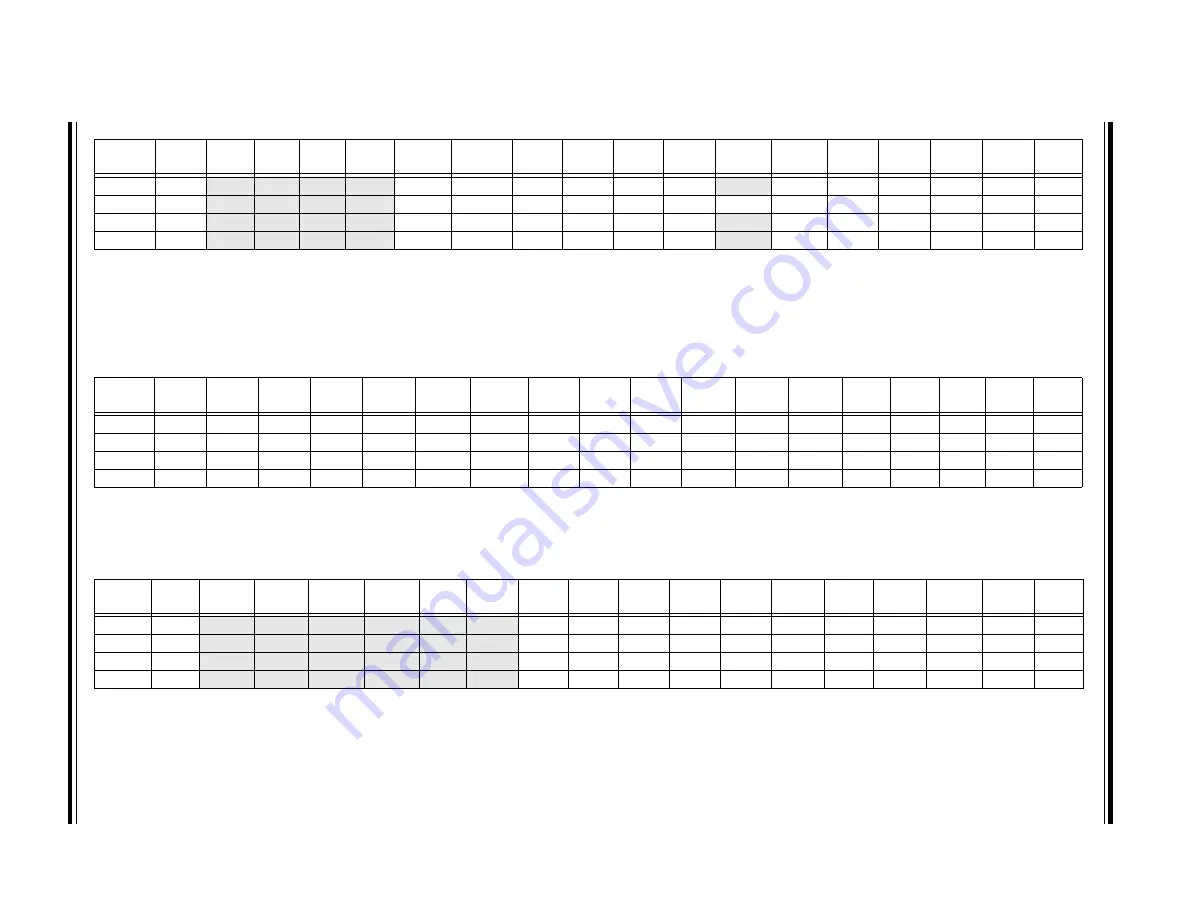
TABLE 4-21:
PORTA REGISTER MAP
File Name
Addr.
Bit 15
Bit 14
Bit 13
Bit 12
Bit 11
Bit 10
)
Bit 9
(
,
)
Bit 8
Bit 7
Bit 6
(
)
Bit 5
(
)
Bit 4
Bit 3
Bit 2
Bit 1
Bit 0
All
Resets
TRISA
2C0h
—
—
—
—
TRISA11
TRISA10
TRISA9
TRISA8
TRISA7
TRISA6
—
TRISA4
TRISA3
TRISA2
TRISA1
TRISA0
0FDF
(
)
PORTA
2C2h
—
—
—
—
RA11
RA10
RA9
RA8
RA7
RA6
RA5
RA4
RA3
RA2
RA1
RA0
xxxx
LATA
2C4h
—
—
—
—
LATA11
LATA10
LATA9
LATA8
LATA7
LATA6
—
LATA4
LATA3
LATA2
LATA1
LATA0
xxxx
ODCA
2C6h
—
—
—
—
ODA11
ODA10
ODA9
ODA8
ODA7
ODA6
—
ODA4
ODA3
ODA2
ODA1
ODA0
0000
Legend:
x
= unknown,
u
= unchanged, — = unimplemented,
q
= value depends on condition, r = reserved.
Bold
indicates shared access SFRs.
Note 1:
Reset value depends on the device type; the PIC24F16KM204 value is shown.
2:
These bits are only available when MCLRE (FPOR<7>) =
0
.
3:
These bits are not implemented in FV devices.
4:
These bits are not implemented in 20-pin devices.
5:
These bits are not implemented in 28-pin devices.
TABLE 4-22:
PORTB REGISTER MAP
File Name
Addr.
Bit 15
Bit 14
Bit 13
Bit 12
Bit 11
(
)
Bit 10
)
Bit 9
Bit 8
Bit 7
Bit 6
(
Bit 5
(
Bit 4
Bit 3
Bit 2
Bit 1
Bit 0
All
Resets
TRISB
2C8h
TRISB15 TRISB14 TRISB13 TRISB12
TRISB11
TRISB10
TRISB9
TRISB8
TRISB7
TRISB6
TRISB5
TRISB4
TRISB3
TRISB2 TRISB1 TRISB0
FFFF
(
PORTB
2CAh
RB15
RB14
RB13
RB12
RB11
RB10
RB9
RB8
RB7
RB6
RB5
RB4
RB3
RB2
RB1
RB0
xxxx
LATB
2CCh
LATB15
LATB14
LATB13
LATB12
LATB11
LATB10
LATB9
LATB8
LATB7
LATB6
LATB5
LATB4
LATB3
LATB2
LATB1
LATB0
xxxx
ODCB
2CEh
ODB15
ODB14
ODB13
ODB12
ODB11
ODB10
ODB9
ODB8
ODB7
ODB6
ODB5
ODB4
ODB3
ODB2
ODB1
ODB0
0000
Legend:
x
= unknown,
u
= unchanged, — = unimplemented,
q
= value depends on condition, r = reserved.
Bold
indicates shared access SFRs.
Note 1:
Reset value depends on the device type; the PIC24F16KM204 value is shown.
2:
These bits are not implemented in 20-pin devices.
TABLE 4-23:
PORTC REGISTER MAP
File
Name
Addr.
Bit 15
Bit 14
Bit 13
Bit 12
Bit 11
Bit 10
Bit 9
(
Bit 8
(
Bit 7
)
Bit 6
(
,
)
Bit 5
(
,
)
Bit 4
(
,
)
Bit 3
Bit 2
)
Bit 1
(
Bit 0
(
,
)
All
Resets
TRISC
2D0h
—
—
—
—
—
—
TRISC9
TRISC8
TRISC7
TRISC6
TRISC5
TRISC4
TRISC3
TRISC2
TRISC1
TRISC0
03FF
(
PORTC
2D2h
—
—
—
—
—
—
RC9
RC8
RC7
RC6
RC5
RC4
RC3
RC2
RC1
RC0
xxxx
LATTC
2D4h
—
—
—
—
—
—
LATC9
LATC8
LATC7
LATC6
LATC5
LATC4
LATC3
LATC2
LATC1
LATC0
xxxx
ODCC
2D6h
—
—
—
—
—
—
ODC9
ODC8
ODC7
ODC6
ODC5
ODC4
ODC3
ODC2
ODC1
ODC0
0000
Legend:
x
= unknown,
u
= unchanged, — = unimplemented,
q
= value depends on condition, r = reserved.
Bold
indicates shared access SFRs.
Note 1:
Reset value depends on the device type; the PIC24F16KM204 value is shown.
2:
These bits are not implemented in 20-pin devices.
3:
These bits are not implemented in 28-pin devices.
Summary of Contents for PIC24FV16KM204 FAMILY
Page 312: ...PIC24FV16KM204 FAMILY DS33030A page 312 Advance Information 2013 Microchip Technology Inc ...
Page 313: ... 2013 Microchip Technology Inc Advance Information DS33030A page 313 PIC24FV16KM204 FAMILY ...
Page 315: ... 2013 Microchip Technology Inc Advance Information DS33030A page 315 PIC24FV16KM204 FAMILY ...
Page 316: ...PIC24FV16KM204 FAMILY DS33030A page 316 Advance Information 2013 Microchip Technology Inc ...
Page 317: ... 2013 Microchip Technology Inc Advance Information DS33030A page 317 PIC24FV16KM204 FAMILY ...
Page 322: ...PIC24FV16KM204 FAMILY DS33030A page 322 Advance Information 2013 Microchip Technology Inc ...


