


2013 Microchip Technology Inc.
Advance Information
DS33030A-page 155
PIC24FV16KM204 FAMILY
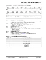
REGISTER 13-5:
CCPxCON3L: CCPx CONTROL 3 LOW REGISTERS
U-0
U-0
U-0
U-0
U-0
U-0
U-0
U-0
—
—
—
—
—
—
—
—
bit 15
bit 8
U-0
U-0
R/W-0
R/W-0
R/W-0
R/W-0
R/W-0
R/W-0
—
—
DT5
DT4
DT3
DT2
DT1
DT0
bit 7
bit 0
Legend:
R = Readable bit
W = Writable bit
U = Unimplemented bit, read as ‘0’
-n = Value at POR
‘1’ = Bit is set
‘0’ = Bit is cleared
x = Bit is unknown
bit 15-6
Unimplemented:
Read as ‘
0
’
bit 5-0
DT<5:0>:
Capture/Compare/PWMx Dead-Time Select bits
111111
= Insert 63 dead-time delay periods between complementary output signals
111110
= Insert 62 dead-time delay periods between complementary output signals
. . .
000010
= Insert 2 dead-time delay periods between complementary output signals
000001
= Insert 1 dead-time delay period between complementary output signals
000000
= Dead-time logic is disabled
Note 1:
This register is implemented in MCCPx modules only.
Summary of Contents for PIC24FV16KM204 FAMILY
Page 312: ...PIC24FV16KM204 FAMILY DS33030A page 312 Advance Information 2013 Microchip Technology Inc ...
Page 313: ... 2013 Microchip Technology Inc Advance Information DS33030A page 313 PIC24FV16KM204 FAMILY ...
Page 315: ... 2013 Microchip Technology Inc Advance Information DS33030A page 315 PIC24FV16KM204 FAMILY ...
Page 316: ...PIC24FV16KM204 FAMILY DS33030A page 316 Advance Information 2013 Microchip Technology Inc ...
Page 317: ... 2013 Microchip Technology Inc Advance Information DS33030A page 317 PIC24FV16KM204 FAMILY ...
Page 322: ...PIC24FV16KM204 FAMILY DS33030A page 322 Advance Information 2013 Microchip Technology Inc ...


