


PIC24FV16KM204 FAMILY
DS33030A-page 156
Advance Information
2013 Microchip Technology Inc.
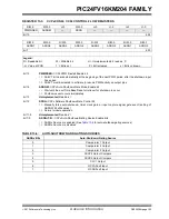
REGISTER 13-6:
CCPxCON3H: CCPx CONTROL 3 HIGH REGISTERS
R/W-0
R/W-0
R/W-0
R/W-0
U-0
R/W-0
R/W-0
R/W-0
OETRIG
OSCNT2
OSCNT1
OSCNT0
—
OUTM2
(
)
OUTM1
(
OUTM0
(
bit 15
bit 8
U-0
U-0
R/W-0
R/W-0
R/W-0
R/W-0
R/W-0
R/W-0
—
—
POLACE
POLBDF
(
PSSACE1
PSSACE0
PSSBDF1
(
PSSBDF0
(
bit 7
bit 0
Legend:
R = Readable bit
W = Writable bit
U = Unimplemented bit, read as ‘0’
-n = Value at POR
‘1’ = Bit is set
‘0’ = Bit is cleared
x = Bit is unknown
bit 15
OETRIG:
Capture/Compare/PWMx Dead-Time Select bit
1
= For Triggered mode (TRIGEN =
1
): module does not drive enabled output pins until triggered
0
= Normal output pin operation
bit 14-12
OSCNT<2:0>:
One-Shot Event Count bits
111
= Extend one-shot event by 7 time base periods (8 time base periods total)
110
= Extend one-shot event by 6 time base periods (7 time base periods total)
101
= Extend one-shot event by 5 time base periods (6 time base periods total)
100
= Extend one-shot event by 4 time base periods (5 time base periods total)
011
= Extend one-shot event by 3 time base periods (4 time base periods total)
010
= Extend one-shot event by 2 time base periods (3 time base periods total)
001
= Extend one-shot event by 1 time base period (2 time base periods total)
000
= Do not extend one-shot Trigger event
bit 11
Unimplemented:
Read as ‘
0
’
bit 10-8
OUTM<2:0>:
PWMx
Output Mode Control bits
(
111
= Reserved
110
= Output Scan mode
101
= Brush DC Output mode, forward
100
= Brush DC Output mode, reverse
011
= Reserved
010
= Half-Bridge Output mode
001
= Push-Pull Output mode
000
= Steerable Single Output mode
bit 7-6
Unimplemented:
Read as ‘
0
’
bit 5
POLACE:
CCPx Output Pins, OCxA, OCxC and OCxE, Polarity Control bit
1
= Output pin polarity is active-low
0
= Output pin polarity is active-high
bit 4
POLBDF:
CCPx Output Pins, OCxB, OCxD and OCxF, Polarity Control bit
)
1
= Output pin polarity is active-low
0
= Output pin polarity is active-high
bit 3-2
PSSACE<1:0>:
PWMx Output Pins, OCxA, OCxC and OCxE, Shutdown State Control bits
11
= Pins are driven active when a shutdown event occurs
10
= Pins are driven inactive when a shutdown event occurs
0x
= Pins are tri-stated when a shutdown event occurs
bit 1-0
PSSBDF<1:0>:
PWMx Output Pins, OCxB, OCxD, and OCxF, Shutdown State Control bits
(
11
= Pins are driven active when a shutdown event occurs
10
= Pins are driven inactive when a shutdown event occurs
0x
= Pins are in a high-impedance state when a shutdown event occurs
Note 1:
These bits are implemented in MCCPx modules only.
Summary of Contents for PIC24FV16KM204 FAMILY
Page 312: ...PIC24FV16KM204 FAMILY DS33030A page 312 Advance Information 2013 Microchip Technology Inc ...
Page 313: ... 2013 Microchip Technology Inc Advance Information DS33030A page 313 PIC24FV16KM204 FAMILY ...
Page 315: ... 2013 Microchip Technology Inc Advance Information DS33030A page 315 PIC24FV16KM204 FAMILY ...
Page 316: ...PIC24FV16KM204 FAMILY DS33030A page 316 Advance Information 2013 Microchip Technology Inc ...
Page 317: ... 2013 Microchip Technology Inc Advance Information DS33030A page 317 PIC24FV16KM204 FAMILY ...
Page 322: ...PIC24FV16KM204 FAMILY DS33030A page 322 Advance Information 2013 Microchip Technology Inc ...


