Installation and Operation
2014 Microchip Technology Inc.
DS50002300A-page 15
2.4
JUMPERS ON THE EVALUATION BOARD
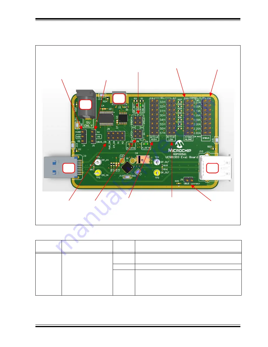
shows the top of the Evaluation Board and highlights the jumpers.
FIGURE 2-3:
Evaluation Board Top View – Jumpers.
TABLE 2-3:
JUMPER DESCRIPTIONS
Designator
Function
Jumper
Position
Description
J4
V
DD
source selection
The jumper populated on this header selects the V
DD
supply source for the digital circuits on the board.
1-2
V
DD
is connected to V
BUS
pin of the J2 USB connector
2-3
V
DD
is connected to V
S
. This is the recommended
configuration when evaluating the Attach Detection feature
of the UCS81003. If the board is evaluated with a PC
running the GUI, then the V
S
must be supplied after the
USB cable is plugged into the J2 connector.
J16
Current Limit,
SMBus mode
J18
Current Limit,
Stand-Alone mode
J8
Connects
UCS81003 V
BUS
output to J10
J9
PWR_EN,
EM_EN,
M1, M2
J17
Address Selection,
PWR_EN Active Low
J19
Address Selection,
PWR_EN Active High
J6
LATCH,
S0
J7
SMBus
data,
clock
J5
V
S
source
selection:
5V from J1 or
from J3 V
BUS
J4
VDD source
selection:
Vs or
V
BUS
from J2
J1
J2
J3
J10


