2-Port USB 2.0 Hi-Speed Hub Controller
Datasheet
2014 Microchip Technology Inc.
DS00001726A-page 9
Chapter 2 Pin Descriptions
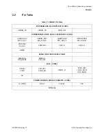
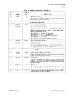
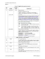
This chapter is organized by a set of pin configurations followed by a corresponding pin list organized
by function according to their associated interface. A detailed description list of each signal (named in
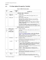
the pin list) is organized by function in
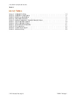
Table 2.2, “USB2422 Pin Descriptions,” on page 11
. Refer to
Table 2.3, “Buffer Type Descriptions,” on page 14
for a list of buffer types.
An
N
at the end of a signal name indicates that the active (asserted) state occurs when the signal is
at a low voltage level. When the
N
is not present, the signal is asserted when it is at a high voltage
level. The terms assertion and negation are used exclusively in order to avoid confusion when working
with a mixture of active low and active high signals. The term assert, or assertion, indicates that a
signal is active, independent of whether that level is represented by a high or low voltage. The term
negate, or negation, indicates that a signal is inactive.
2.1
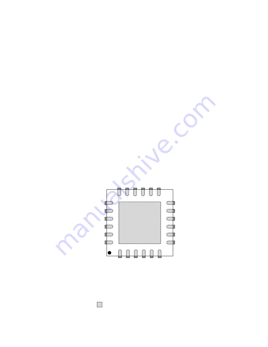
Pin Configuration
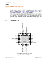
Figure 2.1 USB2422 24-Pin SQFN
Thermal Slug
(must be connected to VSS)
12
11
10
9
8
7
USBDP_UP
19
XTALOUT/(CLKIN_EN)
20
XTALIN/CLKIN
21
RBIAS
24
23
PLLFILT
22
1
VD
D
33
2
US
B
D
P_
DN1
/PRT
_DIS_P1
3
US
B
D
M
_DN
2/
P
R
T_
D
IS_
M
2
4
US
B
D
P_
DN2
/PRT
_DIS_P2
5
6
US
B
D
M
_DN
1/
P
R
T_
D
IS_
M
1
NC
USBDM_UP
17
SU
SP_I
N
D
/L
OCAL_
P
WR
/(NON_R
E
M
0)
16
VB
U
S
_D
E
T
RE
S
E
T
_N
15
14
SM
BC
L
K
/C
FG_
S
EL
0
VD
D
33
18
13
SM
BD
A
T
A/NO
N
_R
E
M1
Indicates pins on the bottom of the device.
OCS1_N
PRTPWR1/(BC_EN1)
VDD33
CRFILT
PRTPWR2
OCS2_N
USB2422
(Top View SQFN-24)

