background image

 2015-2017 Microchip Technology Inc.

DS00001855E-page 23

USB5744

7.0

DEVICE INTERFACES

The USB5744 provides multiple interfaces for configuration and external memory access. This section details the vari-
ous device interfaces and their usage:

SPI Master Interface

SMBus Slave Interface

7.1

SPI Master Interface

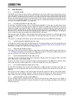
The device is capable of code execution from an external SPI ROM. When configured for SPI Mode, on power up the
firmware looks for an external SPI flash device that contains a valid signature of 

2DFU

 (device firmware upgrade) begin-

ning at address 0xFFFA. If a valid signature is found, then the external ROM is enabled and the code execution begins
at address 0x0000 in the external SPI device. If a valid signature is not found, then execution continues from internal
ROM. 

7.2

SMBus Slave Interface

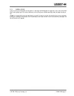
The device includes an integrated SMBus slave interface, which can be used to access internal device run time registers
or program the internal OTP memory. SMBus slave detection is accomplished by detection of pull-up resistors on both
the 

SMDAT

 and 

SMCLK

 signals. Refer to 

Section 3.4.1, "SPI/SMBus Configuration"

 for additional information. 

Note:

For details on how to enable each interface, refer to 

Section 3.4.1, "SPI/SMBus Configuration"

.

For information on device connections, refer to 

Section 4.0, "Device Connections"

. For information on

device configuration, refer to 

Section 6.0, "Device Configuration"

.

Microchip provides a comprehensive software programming tool, Pro-Touch, for configuring the USB5744
functions, registers and OTP memory. All configuration is to be performed via the Pro-Touch programming
tool. For additional information on the Pro-Touch programming tool, refer to Software Libraries within Micro-
chip USB5744 product page at www.microchip.com/USB5744.

Note:

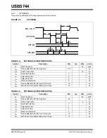
For SPI timing information, refer to 

Section 9.6.7, "SPI Timing"

.

Note:

All device configuration must be performed via the Pro-Touch Programming Tool. For additional information
on the Pro-Touch programming tool, refer to Software Libraries within Microchip USB5744 product page at
www.microchip.com/USB5744.

Summary of Contents for USB5744

Page 1: ...ery Charging rev 1 2 support DCP CDP SDP Apple portable product charger emulation Chinese YD T 1591 2006 charger emulation Chinese YD T 1591 2009 charger emulation European Union universal mobile char...

Page 2: ...mining its literature number found on the bottom outside corner of any page The last character of the literature number is the version number e g DS30000000A is version A of document DS30000000 Errata...

Page 3: ...Preface 4 2 0 Introduction 6 3 0 Pin Description and Configuration 8 4 0 Device Connections 17 5 0 Modes of Operation 19 6 0 Device Configuration 22 7 0 Device Interfaces 23 8 0 Functional Description...

Page 4: ...is not to be confused with the USB Hub Controller that is used to communicate the hub status back to the Host during a USB session I2 C Inter Integrated Circuit LS Low Speed lsb Least Significant Bit...

Page 5: ...SB Engineering Change Notice December 29th 2004 http www usb org 2 Universal Serial Bus Revision 3 1 Specification http www usb org 3 Battery Charging Specification Revision 1 2 Dec 07 2010 http www u...

Page 6: ...g Port Power brick with no data CDP Charging Downstream Port 1 5A with data SDP Standard Downstream Port 0 5A with data Custom profiles loaded via SMBus or OTP Additionally the USB5744 includes many p...

Page 7: ...2015 2017 Microchip Technology Inc DS00001855E page 7 USB5744 FIGURE 2 1 INTERNAL BLOCK DIAGRAM...

Page 8: ...8 19 20 21 22 23 24 25 39 38 37 36 35 34 33 32 53 52 51 50 49 48 47 46 USB3DN_RXDM1 USB3DN_RXDP1 USB2DN_DP2 PRT_DIS_P2 USB2DN_DM2 PRT_DIS_M2 USB3DN_TXDP2 USB3DN_TXDM2 VDD12 USB3DN_RXDP2 SPI_CE_N CFG_N...

Page 9: ...P2 PRT_DIS_P2 36 PRT_CTL1 9 USB2DN_DM2 PRT_DIS_M2 37 VBUS_DET 10 USB3DN_TXDP2 38 SPI_CLK SMCLK 11 USB3DN_TXDM2 39 SPI_DO SMDAT 12 VDD12 40 SPI_DI CFG_BC_EN 13 USB3DN_RXDP2 41 SPI_CE_N CFG_NON_REM 14 U...

Page 10: ...l is inac tive Note The buffer type for each signal is indicated in the Buffer Type column of the pin description tables A description of the buffer types is provided in Section 3 3 Buffer Types on pa...

Page 11: ...IS_M 4 1 for more information See Note 2 1 VBUS_DET IS This signal detects the state of the upstream bus power When designing a detachable hub this pin must be connected to the VBUS power pin of the u...

Page 12: ...es gang mode Gang power pin when used in gang mode TABLE 3 5 SPI SMBUS PIN DESCRIPTIONS Num Pins Symbol Buffer Type Description 1 SPI_CE_N O12 Active low SPI chip enable output GPIO7 I O12 General pur...

Page 13: ...ed 1 XTALO OCLK External 25 MHz crystal output 1 RBIAS AI A 12 0 k 1 resistor is attached from ground to this pin to set the transceiver s internal bias settings 1 ATEST AI Analog test pin This signal...

Page 14: ...signals external to the device When connected to a load that must be pulled high an external resistor must be added PD 50 A typical internal pull down Unless otherwise noted in the pin description int...

Page 15: ...se supported modes are detailed in Table 3 9 The individual pin function assign ments for each mode are detailed in Table 3 10 For additional device connection information refer to Section 4 0 Device...

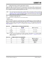
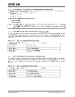
Page 16: ...onfiguration strap is used to configure the battery charging port settings of the device to one of five settings These modes are selected by the configuration of an external resistor on the CFG_BC_EN...

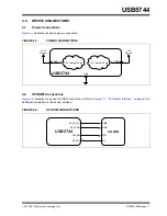
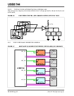
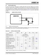
Page 17: ...tions Figure 4 2 illustrates the device SPI ROM connections Refer to Section 7 1 SPI Master Interface on page 23 for additional information on this device interface FIGURE 4 1 POWER CONNECTIONS FIGURE...

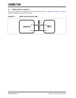
Page 18: ...ve Connections Figure 4 3 illustrates the device SMBus slave connections Refer to Section 7 2 SMBus Slave Interface on page 23 for additional information on this device interface FIGURE 4 3 SMBUS SLAV...

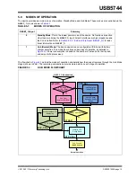
Page 19: ...ng the RESET_N input All port interfaces are high impedance and the PLL is halted Refer to Section 8 2 2 External Chip Reset RESET_N for addi tional information on RESET_N 1 Hub Normal Mode The device...

Page 20: ...FIGURATION READ STAGE CFG_RD In this stage the internal firmware loads the default values from the internal ROM and then uses the configuration strap ping options to override the default values Refer...

Page 21: ...the USB Host on the upstream port The device will remain in the normal mode until the operating mode is changed by the sys tem If RESET_N is asserted low then Standby Mode is entered The device may t...

Page 22: ...t The OTP operates in Single Ended mode For more information refer to the Microchip USB5744 product page and SDK at www microchip com USB5744 6 1 1 2 Battery Charging Access over USB The Battery charg...

Page 23: ...the internal OTP memory SMBus slave detection is accomplished by detection of pull up resistors on both the SMDAT and SMCLK signals Refer to Section 3 4 1 SPI SMBus Configuration for additional inform...

Page 24: ...nal circuitry to actually charge the device Those components must be provided externally by the OEM If the OEM provides an external supply capable of supplying current per the battery charging specifi...

Page 25: ...rn to the default state 4 The external crystal oscillator is halted 5 The PLL is halted 8 2 3 USB BUS RESET In response to the upstream port signaling a reset to the device the device performs the fol...

Page 26: ...ipation the pull up resistor will be disabled at that time When port power is enabled it will disable the output driver and enable the pull up resistor making it an open drain output If there is an ov...

Page 27: ...is an over current situation the poly fuse will open This will cause the cathode of the diode to go to 0 volts The anode of the diode will be at 0 7 volts and the Schmidt trigger input will register...

Page 28: ...E 8 7 USB5744 WITH 4 GENERIC PORT POWER CONTROLLERS 2 BC ENABLED Pull Up Enable USB Device Poly Fuse 5V Pull Up Enable Pull Up Enable 50k 50k 50k PRTPWR OCS USB Device USB Device PRT_CTLx PRT_CTLy PRT...

Page 29: ...enable battery charging on the appro priate ports For example in the application shown in Figure 8 7 CFG_BC_EN must be connected to an external 10 k pull down resistor to enable battery charging on Po...

Page 30: ...ty exists it is suggested to use a clamp circuit Note 2 This rating does not apply to the following pins All USB DM DP pins XTAL1 CLK_IN and XTALO Stresses exceeding those listed in this section could...

Page 31: ...PACKAGE THERMAL PARAMETERS Symbol C W Velocity Meters s JA 30 0 26 1 JT 0 2 0 0 3 1 JC 2 6 0 2 6 1 Note Thermal parameters are measured or estimated for devices in a multi layer 2S2P PCB per JESDN51...

Page 32: ...various modes of operation Power dis sipation is determined by temperature supply voltage and external source sink requirements TABLE 9 3 DEVICE POWER CONSUMPTION Typical mA Typical Power VDD33 VDD12...

Page 33: ...Level High Input Level VIL VIH 2 1 0 9 V V IS Type Input Buffer Low Input Level High Input Level Schmitt Trigger Hysteresis VIHT VILT VIL VIH VHYS 1 9 9 20 0 9 40 V V mV O6 Type Output Buffer Low Outp...

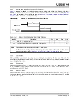
Page 34: ...ation strap values to be read at power on the following timing requirements must be met The operational levels Vopp for the external power supplies are detailed in Section 9 2 Operating Conditions on...

Page 35: ...to the 400KHz Fast Mode Fm voltage power and timing characteristics specifications as set forth in the I2 C Bus Specification Please refer to the I2 C Bus Specification available at http www nxp com d...

Page 36: ...hold time 5 ns tov Clock to output valid 4 ns tcel Chip enable SPI_CE_EN low to first clock 12 ns tceh Last clock to chip enable SPI_CE_EN high 12 ns TABLE 9 9 SPI TIMING 60 MHZ OPERATION Symbol Descr...

Page 37: ...izing matching parallel load capacitors be used for the crystal input output signals XTALI XTALO Refer to Table 9 10 for the recommended crystal specifications Note 6 Frequency Deviation Over Time is...

Page 38: ...PCB capacitance is not included in this value The XTALI CLK_IN pin XTALO pin and PCB capacitance values are required to accurately calcu late the value of the two external load capacitors These two ex...

Page 39: ...n QTP price Legend i Temperature range designator Blank commercial i industrial R Product revision nnn Internal code e3 Pb free JEDEC designator for Matte Tin Sn V Plant of assembly COO Country of ori...

Page 40: ...age 40 2015 2017 Microchip Technology Inc 10 2 Package Drawings Note For the most current package drawings see the Microchip Packaging Specification at http www microchip com packaging FIGURE 10 1 56...

Page 41: ...2015 2017 Microchip Technology Inc DS00001855E page 41 USB5744 FIGURE 10 2 56 VQFN PACKAGE DIMENSIONS...

Page 42: ...USB5744 DS00001855E page 42 2015 2017 Microchip Technology Inc FIGURE 10 3 56 VQFN LAND PATTERN...

Page 43: ...erences to USB 3 1 Gen 1 throughout the document Updated USB specification references Misc typos DS00001855B 04 16 15 Features Changed Environmental feature bullet from 4kV HBM JESD22 A114F ESD protec...

Page 44: ...age 26 Added note under Section 8 4 2 Product Identification System on page 46 Updated ordering information Section 9 1 Absolute Maximum Rat ings on page 30 Updated 1 2V supply voltage absolute max va...

Page 45: ...p sales offices distributors and factory representatives CUSTOMER CHANGE NOTIFICATION SERVICE Microchip s customer notification service helps keep customers current on Microchip products Subscribers w...

Page 46: ...roller disabled Examples a USB5744 2G Tray Commercial temp 56 pin VQFN b USB5744 I 2G Tray Industrial temp 56 pin VQFN c USB5744T I 2G Tape reel Industrial temp 56 pin VQFN d USB5744T 2G Tape reel Com...

Page 47: ...SHARC USBCheck VariSense ViewSpan WiperLock Wireless DNA and ZENA are trademarks of Microchip Technology Incorporated in the U S A and other countries SQTP is a service mark of Microchip Technology In...

Page 48: ...6 27 5980 5118 China Xian Tel 86 29 8833 7252 Fax 86 29 8833 7256 ASIA PACIFIC China Xiamen Tel 86 592 2388138 Fax 86 592 2388130 China Zhuhai Tel 86 756 3210040 Fax 86 756 3210049 India Bangalore Tel...

Reviews: