Interfaces 6
miriac EK-5744 User Manual
V 1.2
42/53
© MicroSys Electronics GmbH 2017
6.6.2 First Stage Specification
The first stage load switches are current limited, short-circuit and over-temperature
protected.
A single first stage switch is able to deliver more than 1A into the four output
drivers, which allows for a specification of 0.25A per output according to IEC61131-
2 table 9.
The short current and shutdown time specification of the first stage driver is shown
in the following figure:
The load switch has a delay of 250us which must be taken into account for the
status verification.
For testing the first stage without disturbing active outputs the following sequence
must be performed. We assume that stage AB is active at step 1.
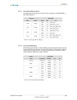
6.6.2.1
First Stage AB/CD Enable
Enable
MPC5744P
Signal
Stage
Pin
Name
PWENA#
First Stage AB
B14
Port C10
PWENB#
First Stage AB
E15
Port C13
PWENC#
First Stage CD
C6
Port I0
PWEND#
First Stage CD
D11
Port I2
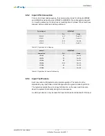
Table 6-11: Digital Output First Stage Enable Pin Mapping
6.6.2.2
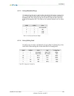
Read Back Status
The read back value of both first stage status lines must be identical.
A low value indicates an active first stage switch.
Figure 6-8: First Stage Switch Timing Specification

