miriac SBC-S32G-R3_User Manual
V 3.2
43/65
© MicroSys Electronics GmbH 2021
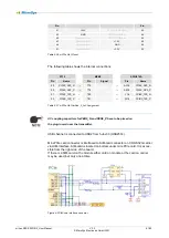
The following table shows the internal connections:
ST9
MXM1
S32G274A
Pin
Name
Pin
Signal
Pin
Name
43
M2_TX0_P
→
T85
←
W19
PCIE1_TX0_P
41
M2_TX0_N
→
T84
←
Y18
PCIE1_TX0_N
49
M2_RX0_P
←
T70
→
AA22
PCIE1_RX0_P
47
M2_RX0_N
←
T69
→
AB22
PCIE1_RX0_N
Table 6-29 M.2 M-key Slot SerDes_1_Ln0 Assignment
6.5.3 PCIe Root Complex / Endpoint
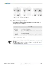
Switch SW2-3 can be used to change the configuration of the SBC-S32G274A
from “Root Complex” to “Endpoint”.
Table 6-30 PCIe Root Complex / Endpoint
It is also necessary to adapt the software configuration of the two systems involved in
the setup.
By setting the “Endpoint” mode without correct software configuration the behaviour
of the SBC-S32G274A may be unpredictable.
Mode
Description
„Root Complex“
(standard)
SW2-3 off
The SoM is a PCIe Root Complex.
The SBC-S32G274A drives PCIe lanes and controls reset and clock to any
PCIe card plugged in ST15
„Endpoint“
SW2-3 on
The SoM is a PCIe Endpoint.
The SBC-S32G274A expects to be controlled by any PCIe Root Complex
connected via ST15. This includes reset, clock and PCIe lanes.


