background image


System Description 4 


miriac SBC-S32V User Manual 

V 1.1 

30/81 


© MicroSys Electronics GmbH 2017 


4.15.7  MIPI Power 

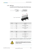
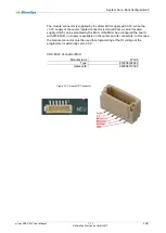
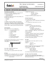
The two MIPI ports of the SBC-S32V system can be either work with 5.0V only or 
mixed with +5.0V and +12V. This option is handled by two 5 pin 2.54mm headers. 


Manufacturer: 

Fischerelektronik 

Type: 

SL10SMD0525G 

mates with:  

2.54mm Jumper Link 


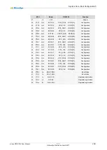
PWA 

Signal


Description 

+5.0V 

Power Rail 

VCCA 

Supply for MIPIA Pin 25 & 27 

GND 

Ground 

VCCA 

Supply for MIPIA Pin 25 & 27 

+12V 

Power Rail 


PWB 

Signal


Description 

+5.0V 

Power Rail 

VCCB 

Supply for MIPIB Pin 25 & 27 

GND 

Ground 

VCCB 

Supply for MIPIB Pin 25 & 27 

+12V 

Power Rail 

In case the pins 25 and 27 should not be powered, no link at all should be installed. 
If these pins should be grounded, a link between pin 2 and 3 or 3 and 4 must be 
set.  


Anyway, only a single link per header must be set at a 
time. More than one link installed may cause permanent 
damage to the board! 


Figure 15: Header PWA & PWB


Summary of Contents for miriac SBC-S32V

Page 1: ...Creating Embedded Systems miriac SBC S32V User Manual V 1 1...

Page 2: ...om Side 22 4 14 System Environment 23 4 14 1 Temperature Ratings 23 4 14 2 Power Dissipation 25 4 15 Power Supply 26 4 15 1 Input Supply Rating 26 4 15 2 Input Power Connector 26 4 15 3 Input Power Sw...

Page 3: ...Manual V 1 1 3 81 MicroSys Electronics GmbH 2017 9 7 1 CAN0 71 9 7 2 CAN1 71 9 7 3 Termination 72 9 8 LEDs 73 9 9 Switches 74 9 10 Jumpers 76 10 Appendix 77 10 1 Acronyms 77 10 2 Table of Figures 78...

Page 4: ...issions in this document MicroSys Electronics GmbH neither gives any guarantee nor accepts any liability whatsoever for consequential damages resulting from the use of this manual or its associated pr...

Page 5: ...shipment which is dependent on the preferred carrier and the location where you want to have it shipped to by sending a request to MicroSys Electronics GmbH Muehlweg 1 D 82054 Sauerlach Germany In yo...

Page 6: ...and its features Table 1 Symbols 1 5 2 Conventions Symbol explanation denotes a low active signal denotes the signal flow in the shown direction denotes the signal flow in the shown direction denotes...

Page 7: ...it may become hot during operation Take care not to touch any parts of the circuitry during operation to avoid burns and operate the unit in a well ventilated location Provide an appropriate cooling s...

Page 8: ...rd It targets both evaluation of the MPX S32V SOM direct usage as an industrial ADAS computing solution This document provides you an overview on the system devices connectors and functions and how to...

Page 9: ...the following items an adequate power supply delivering 12V DC stabilized 2 A min an USB cable type A micro B adapted to connector USB a serial terminal such as a PC with an USB port running a termin...

Page 10: ...ch Make sure the switch BMD located on the MPX S32V module is set properly in order to select the correct boot source For more details see chapter 5 2 Boot Mode Configuration Make sure the switch GPU...

Page 11: ...the power switch PWR is in off position released Connect the 12V power line to the PWRA connector Switch on the power by switch PWR After Power On the green LED on the carrier should light up IF NOT...

Page 12: ...will start On startup U Boot will come up similar to the following The exact output may vary depending on U Boot and MPX S32V module versions in use U Boot 2016 01 Aug 04 2017 09 06 53 0200 CPU NXP S...

Page 13: ...4 miriac SBC S32V User Manual V 1 1 13 81 MicroSys Electronics GmbH 2017 4 System Description This section describes all parts of the SBC S32V system 4 1 Block Diagram CRX S32V Carrier 4 2 Block Diagr...

Page 14: ...hy 10 100 1000 BaseT Link Activity Leds Grahics Output TFP410 HDMI Type A DDC support Video Input MIPI CSI A 5V 12V supply 4 Lanes Clock 27MHz Ref Clock Mounting Holes MIPI CSI B 5V 12V supply 4 Lanes...

Page 15: ...MI Out MIPI A MIPI B CAN A CAN B LIN Interface JTAG Indicators Module Leds MCU Status Reset Status User GPIO1 User GPIO2 Carrier Leds 12V Power Indicator User Led 1 User Led 2 Debug JTAG 10 pin Header...

Page 16: ...tig Holes 2 5mm all electrically floating Carrier Mounting 4 Mountig Spacers M2 5 2 Holes electrically floating 2 Holes electrically grounded miniPCIe Mounting 2 Mounting Spacers M2 5 all electrically...

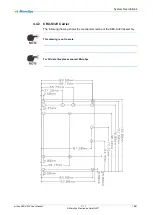
Page 17: ...GmbH 2017 4 4 Mechanical Dimensions 4 4 1 MPX S32V Module The following drawing shows the mechanical outline of the MPX S32V module that is plugged in the CRX S32V carrier board This drawing is not t...

Page 18: ...S32V User Manual V 1 1 18 81 MicroSys Electronics GmbH 2017 4 4 2 CRX S32V Carrier The following drawing shows the mechanical outline of the SBC S32V assembly This drawing is not to scale For 3D data...

Page 19: ...System Description 4 miriac SBC S32V User Manual V 1 1 19 81 MicroSys Electronics GmbH 2017 4 5 Carrier Board Layout Module Side Figure 9 Module Side connectors carrier CRX S32V...

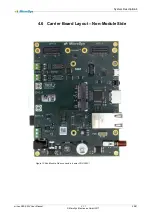
Page 20: ...System Description 4 miriac SBC S32V User Manual V 1 1 20 81 MicroSys Electronics GmbH 2017 4 6 Carrier Board Layout Non Module Side Figure 10 Non Module Side connectors carrier CRX S32V...

Page 21: ...escription 4 miriac SBC S32V User Manual V 1 1 21 81 MicroSys Electronics GmbH 2017 4 7 Carrier Power Button Side View 4 8 Carrier Power Plug Side View 4 9 Carrier Bottom Side View 4 10 Carrier Top Si...

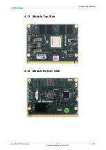
Page 22: ...System Description 4 miriac SBC S32V User Manual V 1 1 22 81 MicroSys Electronics GmbH 2017 4 11 Module Top Side 4 12 Module Bottom Side...

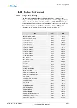
Page 23: ...2MFR 1BL 30 C 70 C BAT HOLDER 79527141 55 C 85 C C 0402 NP0 Series 55 C 125 C C 0402 X5R Series 55 C 85 C C 0402 X7R Series 55 C 125 C C 0603 226 X5R Z 55 C 85 C C 0603 X7R Series 55 C 125 C C 0805 X7...

Page 24: ...383 56033 40 C 85 C L 744 383 57068 40 C 85 C L 744 771 001 55 C 125 C LD 155124xx73200 40 C 85 C PCB ADP 8065 01 40 C 85 C PCB CRX S32V 01 40 C 85 C PCB MPX S32V 02 40 C 85 C PTC 2920L330 24 40 C 85...

Page 25: ...C 150 C T FDT434P 55 C 150 C T PDTA114YT 55 C 150 C T PDTC123JT 65 C 150 C TVS 1 5SMC15AT3 65 C 150 C TVS ESD7504MUTAG 55 C 125 C TVS PSOT36LC 55 C 150 C TVS USBLC6 2P6 40 C 125 C XT FT13A xx 00000 8...

Page 26: ...tion 12V room temperature U boot prompt 0 40A The input of the SBC S32V system is protected against wrong polarity and over current DO NOT exceed the rated maximum values for the power supply This may...

Page 27: ...an on state resistance of 100mR and it is fully protected against current and thermal overload The push button switch has two alternate positions i e pressed and released The position of the switch s...

Page 28: ...a self resettable fuse with a nominal current rating of 3 3A at 20 C ambient temperature The current is derated due to the ambient temperature according to the following table 40 C 20 C 0 C 20 C 40 C...

Page 29: ...miniPCIe modules The current rating is limited to 1A per pin The voltages are switched on and off by the main power switch The 12V voltage is sourced by the input voltage which is derated by maximal 5...

Page 30: ...0V Power Rail 2 VCCA Supply for MIPIA Pin 25 27 3 GND Ground 4 VCCA Supply for MIPIA Pin 25 27 5 12V Power Rail PWB Signal Description 1 5 0V Power Rail 2 VCCB Supply for MIPIB Pin 25 27 3 GND Ground...

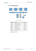
Page 31: ...e for the whole system which is at least 100ms long As long the reset key is pressed the system will be held in the reset state If the key is released the CPU will fetch its power up configuration and...

Page 32: ...lobal Reset Input 4K7 Pullup RSTOUT System Global Reset Output Totem Pole PORST Power On Reset for CPU Totem Pole RESET Reset for CPU Open Drain FRSTI Reset for eMMC device Totem Pole M0RST Reset for...

Page 33: ...oSys Electronics GmbH 2017 5 System Core Boot Configuration 5 1 Processor NXP S32V234 The S32V234 is a vision processing MPU with four ARM Cortex A53 cores and a single Cortex M4 core The four CPU cor...

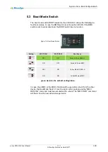
Page 34: ...configuration Note 1 BMD0 and BMD1 are soldered resistors size 0402 and not intended to be changed by user Shown positions set the according BTMOD0 1 line to low BTMOD0 controls the CPU configuration...

Page 35: ...e BOOT switch has no function Setting BOOT SEL1 BOOT SEL2 Boot Device OFF OFF Cortex A53 via SDHC A ON OFF Cortex A53 via eMMC OFF ON Cortex M4 via SDHC A ON ON Cortex M4 via eMMC green denotes the de...

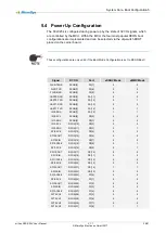
Page 36: ...2 PA 9 0 0 UART0 RXD RCON 3 PA 11 0 0 UART0 TXD RCON 4 PA 12 0 1 UART1 RXD RCON 5 PA 13 0 0 UART1 TXD RCON 6 PA 14 0 1 I2C0 SDA RCON 7 PA 15 1 1 I2C0 SCL RCON 8 PB 0 0 0 I2C1 SDA RCON 9 PB 1 0 0 I2C1...

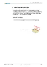
Page 37: ...ates supply voltages and drives all configuration lines of the S32V234 CPU The controller can be either programmed via a module connector or a connector on the carrier board both named MCU As the modu...

Page 38: ...or is derived from a carrier located supply which can be disabled by the MCU If the MCU has configured the board with PWEN off no supply is available on the carrier and its connectors In this case the...

Page 39: ...PowerOnReset 18 PTB5 Out RESET RESET Reset 19 PTB4 In FCCU F0 FCCU_F0 Failure Check Correction 20 PTC3 In LD4 yellow Led 21 PTC2 In 3V3 ADC Divider 3 4 22 PTD7 Out NMI NMI Interrupt 23 PTD6 Out FCCU...

Page 40: ...SPI1_SOUT RCON 17 Configuration 50 PTA0 Out BCFG31 FXT0_CH3 RCON 31 Configuration 51 PTC7 Out BCFG26 SPI3_SIN RCON 26 Configuration 52 PTC6 Out BCFG30 FXT0_CH2 RCON 30 Configuration 53 PTE3 Out BCFG1...

Page 41: ...Torx screws M2 5x16 The SBC S32V is designed to stand in an upright position with the two MIPI camera connectors on top and the heatsink as vertical support The recess at the bottom of the heatsink a...

Page 42: ...To mount the MPX S32V module make sure that the carrier is disconnected from any power or other IO interfaces Both connector surfaces of the module must be clean as well as the carrier connector shoul...

Page 43: ...Now check the gap between carrier and module for other parts than the CPU touching the heatsink Check the thermal CPU pad for correct position Tighten the four screws with no more than 30Ncm For the r...

Page 44: ...bus is actively terminated and the routed in a fly by structure The following table shows all trace lengths in case write leveling should be adjusted The used layer stack together with the FR4 materia...

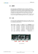
Page 45: ...MMC device is connected to port PTB7 of the MCU In case this port is not configured the FRSTI signal is tied to 3 3V by a pullup resistor 6 4 Leds There are four LEDs onboard the MPX S32V module The u...

Page 46: ...GPU is not used The other sliding switch BMD is used to select between RCON controlled and serial boot mode Both switches are located at the PCB edge on the bottom of the MPX S32V module Any handling...

Page 47: ...s GmbH 2017 6 6 Module Connector The carrier board CRX S32V provides a connector MXM which accepts only compatible CPU modules from the MicroSys MPX S32V family Manufacturer JAE Type MM70 314 310 B1 1...

Page 48: ...G TMS JTAG T7 GND T7 GND B8 GND B8 GND T8 CSI1 DT0 1 0V T8 CSI1 DT0 MIPIB B9 JTAG TDO 3 3V B9 JTAG TDO JTAG T9 CSI1 DT0 1 0V T9 CSI1 DT0 MIPIB B10 FLXR TENB 3 3V B10 FLXR TENB CAN1 T10 GND T10 GND B11...

Page 49: ...D T28 GND B29 VIU0 D08 3 3V 1 8V B29 T29 VIU0 D19 3 3V 1 8V T29 B30 VIU0 D09 3 3V 1 8V B30 T30 VIU0 D20 3 3V 1 8V T30 B31 GND B31 GND T31 GND T31 GND B32 VIU0 D10 3 3V 1 8V B32 T32 VIU0 D21 3 3V 1 8V...

Page 50: ...1 8V B53 T53 DCU DE 1 8V T53 DCU DE HDMI B54 VIU1 D20 3 3V 1 8V B54 T54 DCU PCLK 1 8V T54 DCU PCLK HDMI B55 GND B55 GND T55 GND T55 GND B56 VIU1 D21 3 3V 1 8V B56 T56 DCU HSYNC 1 8V T56 DCU HSYNC HDM...

Page 51: ...B76 GND B76 GND T76 GND T76 GND B77 SDHC CLK 3 3V B77 SDHC CLK SDHC A T77 SDHC D2 3 3V T77 SDHC D2 SDHC A B78 SDHC WP 3 3V B78 SDHC WP SDHC A T78 SDHC D1 3 3V T78 SDHC D1 SDHC A B79 GND B79 GND T79 GN...

Page 52: ...SIN 1 8V B99 CSI0 SYN MIPIA T99 GND T99 GND B100 SPI1 SOUT 1 8V B100 CSI1 SYN MIPIB T100 EC COL 1 8V T100 EC COL LAN B101 GND B101 GND T101 EC TXCK 1 8V T101 EC TXCK LAN B102 SPI1 SCK 1 8V B102 T102...

Page 53: ...T120 GND B121 TRACE D02 1 8V B121 T121 EC RXCK 1 8V T121 EC RXCK LAN B122 TRACE D04 1 8V B122 T122 EC TXD1 1 8V T122 EC TXD1 LAN B123 TRACE D06 1 8V B123 T123 GND T123 GND B124 GND B124 GND T124 TRAC...

Page 54: ...B141 GND T141 GND T141 GND B142 GND B142 GND T142 GND T142 GND B143 GND B143 GND T143 GND T143 GND B144 GND B144 GND T144 GND T144 GND B145 GND B145 GND T145 GND T145 GND B146 GND B146 GND T146 VIN T1...

Page 55: ...an ARM interface on a 2x5 pin header Pin 7 of this header usually connects the return clock RTCK and is not used on the CRX S32V For boundary scan purposes it can be used to control the TRST signal As...

Page 56: ...ut Reference voltage 2 TMS D9 TMS LVTTL Input Test mode select 4k7 pullup to 3 3V 3 GND LVTTL Ground 4 TCK B9 TCK LVTTL Input Clock 4k7 pullup to 3 3V 5 GND LVTTL Ground 6 TDO E10 TDO LVTTL Output Dat...

Page 57: ...le access address of HDMI and miniPCIe slot devices care must be taken to avoid double addressing with the other I C devices on this bus 8 1 1 Bus Map I C Bus 0 Address Reference Device Function 0x00...

Page 58: ...e a nominal voltage of 3 0V The backup battery is necessary to keep time and date of the real time clock on the MPX S32V module Manufacturer W rth Type 79527141 Used with CR2032 batteries 3V 8 1 3 Dig...

Page 59: ...fore the port PH11 must be configured as general purpose output The hot plug detect feature of the HDMI interface is supported by the TFP410 transmitter through its I C CTL_2_MODE register The TFP410...

Page 60: ...a Pair 2 4 TMDS D1 Data Pair 1 5 TMDS Shield Data Pair 1 Shield 6 TMDS D1 Data Pair 1 7 TMDS D0 Data Pair 0 8 TMDS Shield Data Pair 0 Shield 9 TMDS D0 Data Pair 0 10 TMDS Clock Clock Pair 11 TMDS Shie...

Page 61: ...RNX netphy It works with a RGMII connection and responds on the management address 0x01 The LAN jack contains two LEDs to indicated the actual link and transmit status The following picture shows the...

Page 62: ...upplied with 3 3V and 1 5V Additional voltages like 5 0V or 12V are accessible by the power connector PWE1 located between power switch and LAN connector The power rating for this connector is max 1A...

Page 63: ...11 REFCLK UIM CLK 12 13 REFCLK UIM RST 14 15 GND UIM VPP 16 MECHANICAL KEY 17 Reserved GND 18 19 Reserved WDIS 20 21 GND PERST 22 23 PER0 3 3V 24 25 PER0 GND 26 27 GND 1 5V 28 29 GND I C2 SCL 30 31 P...

Page 64: ...meras using Maxim deserializers Both interfaces are supplied with 5 0V and can be configured also for a 12V supply via the two headers PWA and PWB For more information about the power setting for MIPI...

Page 65: ...Peripherals 9 miriac SBC S32V User Manual V 1 1 65 81 MicroSys Electronics GmbH 2017 9 4 1 MIPI Connectors Manufacturer Samtec Type QSE 020 01 F D mates with QTE 020 01 F D...

Page 66: ...d 13 CSI0 SCL 1 8V I C Bus 0 PG4 14 CSI0 DT0 1 0V MIPI Lane 0 15 n c 16 CSI0 DT0 1 0V MIPI Lane 0 17 n c 18 GND Reference Ground 19 n c 20 CSI0 CLK 1 0V MIPI Clock 21 CSI0 RST 1 8V Reset Line PC6 22 C...

Page 67: ...13 CSI1 SCL 1 8V I C Bus 1 PG6 14 CSI1 DT0 1 0V MIPI Lane 0 15 n c 16 CSI1 DT0 1 0V MIPI Lane 0 17 n c 18 GND Reference Ground 19 n c 20 CSI1 CLK 1 0V MIPI Clock 21 CSI1 RST 1 8V Reset Line PB15 22 C...

Page 68: ...ounting option and not installed in the standard version Manufacturer Yamaichi Type PJS 008 2130 0 Used with microSD cards microSD card slot A interconnection I O Range SDHCA S32V234 Pin Name Pin Sign...

Page 69: ...SDHCA S32V234 Pin Name Pin Signal Port LVTTL 1 DAT2 N20 SD_DAT2 PF5 LVTTL 2 CD DAT3 N25 SD_DAT3 PF6 LVTTL 3 CMD P22 SD_CMD PF2 4 Vdd LVTTL 5 CLK P21 SD_CLK PF1 6 Vss LVTTL 7 DAT0 M20 SD_DAT0 PF3 LVTT...

Page 70: ...to USB 2 0 for easy console port connection with a PC UART2 is converted to the LIN 2 1 standard and available on a three terminal wire connector 9 6 1 UART1 Manufacturer W rth Elektronik Type 629 105...

Page 71: ...cessible via two 2 terminal wire connectors The necessary 120 ohms end point termination can be activated by two dip switches 9 7 1 CAN0 Manufacturer W rth Elektronik Type 691 214 110 002 Mates with 0...

Page 72: ...nd the terminal blocks It is activated if the according dip switch is set to ON Manufacturer W rth Elektronik Type 416131160802 Setting TERM 1 TERM 2 CAN0 CAN1 OFF OFF no termination no termination ON...

Page 73: ...onnector is connected to the CPU port PA8 and the red user led directly under the LAN jack uses CPU port PA9 The ethernet LEDs are integrated into the RJ45 jack and indicate link status and traffic Le...

Page 74: ...es BOOT and BMD the CAN termination switch TERM and the GPU power enable switch The power switch is an alternate action pushbutton switch to enable or disable power on all power rails for the whole sy...

Page 75: ...CAN termination switch is used to enable or disable a 120R termination resistor for each CAN line For more information refer to 9 7 3 Termination The GPU power enable switch is used to reduce power co...

Page 76: ...cks onboard the SBC S32V Two 5 pin headers for MIPI power selection Anyway only a single link per header must be set at a time More than one link installed may cause permanent damage to the board One...

Page 77: ...D Electrostatic Discharge FR4 flame retardant 4 GND Ground GPIO General Purpose IO GPL General Public License GPU Graphic Processing Unit HDMI High Definition Multimedia Interface I C Inter Integrated...

Page 78: ...on BTM0 low 34 Figure 18 Position BTM1 low 34 Figure 19 Boot Mode Switch 35 Figure 20 Module MCU Connector 37 Figure 21 Carrier MCU Connector 38 Figure 22 MPX Leds 45 Figure 23 GPU switch 46 Figure 24...

Page 79: ...ppendix 10 miriac SBC S32V User Manual V 1 1 79 81 MicroSys Electronics GmbH 2017 Figure 45 Carrier Leds 73 Figure 46 MIPI A Power Selection 76 Figure 47 MIPI B Power Selection 76 Figure 48 JRS Link 7...

Page 80: ...6 Table 3 Safety and Handling Precautions 7 Table 4 MXM Connector 54 Table 5 JTAG Header 55 Table 6 I C0 bus map 57 Table 7 I C1 bus map 57 Table 8 I C2 bus map 57 Table 9 DDC Function 59 Table 10 mi...

Page 81: ...y Date Version Change Description 2017 07 26 1 0 Initial Release Version preliminary 2017 08 01 1 01 MIPI Chapter and Rev 2 photos added 2017 09 01 1 1 Some review inputs implemented Typos corrected D...

Reviews: