miriac SBC-S32V234 User Manual
V 1.0
25/40
© MicroSys Electronics GmbH 2018
5.2
DRAM
The module is fitted with two individual DDR3L memory blocks, each 32-bit wide
and with 1GByte capacity. The parts used are 4Gbit devices organized in 256M x
16 bits with 15 row, 10 column and 3 bank addresses. The refresh rate depends on
the operating temperature must be set according to the following table
Case Temperature
Refresh Cycle Time
Tc<85°C
7.8us
85°C<Tc<95°C
3.9us
95°C<Tc<105°C
1.95us
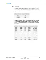
The DDR3L command bus is actively terminated and routed in a fly-by topology.
The following table shows all trace lengths, in case write leveling needs to be
adjusted. The layer stack, together with the FR4 material, causes a signal delay
time of 6.8ps/mm.
DRAM
Signal Group
Trace Length
Description
Bank0
Command
J1->J2
54.0mm
CPU->DRAM
Bank0
Command
J2->J3
13.1mm
DRAM->DRAM
Bank0
Byte 0
J1->J2
25.7mm
CPU->DRAM
Bank0
Byte 1
J1->J2
22.7mm
CPU->DRAM
Bank0
Byte 2
J1->J3
23.1mm
CPU->DRAM
Bank0
Byte 3
J1->J3
18.3mm
CPU->DRAM
Bank1
Command
J1->J4
54.5mm
CPU->DRAM
Bank1
Command
J4>J5
13.9mm
DRAM->DRAM
Bank1
Byte 0
J1->J4
25.3mm
CPU->DRAM
Bank1
Byte 1
J1->J4
22.9mm
CPU->DRAM
Bank1
Byte 2
J1->J5
19.0mm
CPU->DRAM
Bank1
Byte 3
J1->J5
17.2mm
CPU->DRAM

