background image


miriac SBC-S32V234 User Manual 

V 1.0 

4/40 


© MicroSys Electronics GmbH 2018 


1.5 

Symbols, Conventions and Abbreviations 

1.5.1  Symbols 

Throughout this document, the following symbols will be used: 


Information marked with this symbol MUST be obeyed to 
avoid the risk of severe injury, health danger, or major 
destruction of the unit and its environment 


Information marked with this symbol MUST be obeyed to 
avoid the risk of possible injury, permanent damage or 
malfunction of the unit. 


Information marked with this symbol gives important hints 
upon details of this manual, or in order to get the best use 
out of the product and its features. 


Table 1 Symbols 

1.5.2  Conventions 


Symbol 

explanation 

#  

denotes a low active signal  

←  

denotes the signal flow in the shown direction  

→  

denotes the signal flow in the shown direction  

↔  

denotes the signal flow in both directions  

→ 


denotes the signal flow in the shown direction with additional logic / 
additional ICs in the signal path 

I/O  

denotes a bidirectional pin  

Input  

denotes an input pin  

matched  

denotes the according signal to be routed impedance controlled and 
length matched  

Output  

denotes an output pin  

Pin 1  

refers to the numeric pin of a component package  

Pin a1  

refers to the array position of a pin within a component package  

XXX-  

denotes the negative signal of a differential pair  

XXX+  

denotes the positive signal of a differential pair  

XXX  

denotes an optional not mounted or fitted part  

Table 2 Conventions 

Summary of Contents for miriac SBC-S32V234

Page 1: ...Creating Embedded Systems miriac SBC S32V234 User Manual V 1 0...

Page 2: ...ns in this document MicroSys Electronics GmbH neither gives any guarantee nor accepts any liability whatsoever for consequential damages resulting from the use of this manual or its associated product...

Page 3: ...ment which is dependent on the preferred carrier and the location where you want to have it shipped to by sending a request to MicroSys Electronics GmbH Muehlweg 1 82054 Sauerlach Germany In your requ...

Page 4: ...s features Table 1 Symbols 1 5 2 Conventions Symbol explanation denotes a low active signal denotes the signal flow in the shown direction denotes the signal flow in the shown direction denotes the si...

Page 5: ...t during operation Take care not to touch any parts of the circuitry during operation to avoid burns and operate the unit in a well ventilated location Provide an appropriate cooling solution as requi...

Page 6: ...V234 SoM NXP S32V234 1GHz CPU 2GB DDR3L standard temp 0C to 70C 854902 miriac MPX S32V234 SoM same as 854901 but with extended temp 40C to 70C 854903 miriac MPX S32V234 SoM same as 854901 except CPU c...

Page 7: ...nt the module on your own carrier then you will need to modify U Boot accordingly The SBC S32V234 which is the MPX S32V234 module mounted on the CRX 32V carrier is supported by NXP s automotive Linux...

Page 8: ...miriac SBC S32V234 User Manual V 1 0 8 40 MicroSys Electronics GmbH 2018 3 Module Description This section describes all parts of the MPX S32V234 module 3 1 Block Diagram MPX S32V234 Module...

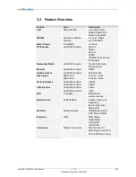
Page 9: ...4 8 bit support Ethernet via MXM Connector RGMII Grahics Output via MXM Connector Parallel 24 bit Video Input MIPI CSI A 4 Lanes Clock MIPI CSI B 4 Lanes Clock Serial Interfaces via MXM Connector UART...

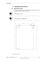
Page 10: ...3 Mechanical Dimensions 3 3 1 MPX S32V234 Module The following drawing shows the mechanical outline of the MPX S32V234 module that is plugged into the CRX S32V carrier board This drawing is not to sca...

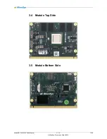
Page 11: ...miriac SBC S32V234 User Manual V 1 0 11 40 MicroSys Electronics GmbH 2018 3 4 Module Top Side 3 5 Module Bottom Side...

Page 12: ...0805 X7R Series 55 C 125 C C 1206 X7R Series 55 C 125 C C EEEFK1H331AQ 55 C 105 C CML 744 227 40 C 125 C CML 744 233 670 40 C 85 C D B320A 13 F 55 C 150 C D BAS70 65 C 150 C D BAT54S 55 C 125 C D SD21...

Page 13: ...xx73200 40 C 85 C PCB ADP 8065 01 40 C 85 C PCB MPX S32V234 02 40 C 85 C R 0402 Serie 55 C 155 C R 0603 Serie 55 C 155 C R 0805 Serie 55 C 155 C R 1206 Serie 55 C 155 C R 2010 Serie 55 C 155 C ST WE 6...

Page 14: ...h the following ratings Input Voltage Operating Range 12V DC 25 Typical Current Consumption room temperature U Boot prompt 0 40A 12V The input of the MPX S32V234 system is not protected against wrong...

Page 15: ...T will be released after 100ms A low level on the RSTIN line extends this time During normal operation a falling edge at RSTIN initiates a reset sequence for the whole system which is at least 100ms l...

Page 16: ...N System Global Reset Input 4K7 Pullup RSTOUT System Global Reset Output Totem Pole PORST Power On Reset for CPU Totem Pole RESET Reset for CPU Open Drain M0RST Reset for Memory Bank 0 Totem Pole M1RS...

Page 17: ...s GmbH 2018 4 System Core Boot Configuration 4 1 Processor NXP S32V234 The S32V234 is a vision processing MPU with four ARM Cortex A53 cores and a single Cortex M4 core The four CPU cores run at a max...

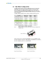
Page 18: ...guration Note 1 BMD0 and BMD1 are soldered resistors size 0402 and not intended to be changed by user Shown positions set the corresponding BTMOD0 1 line to low BTMOD0 controls the CPU configuration p...

Page 19: ...switch is set to serial download these signals have no function If the eMMC or the SDHC are to be used after previously having booted from the other device then BOOT SEL1 must be set correctly and the...

Page 20: ...0 RXD RCON 3 PA 11 0 0 UART0 TXD RCON 4 PA 12 0 1 UART1 RXD RCON 5 PA 13 0 0 UART1 TXD RCON 6 PA 14 0 1 I2C0 SDA RCON 7 PA 15 1 1 I2C0 SCL RCON 8 PB 0 0 0 I2C1 SDA RCON 9 PB 1 0 0 I2C1 SCL RCON 10 PB...

Page 21: ...lines of the S32V234 CPU The controller can be either programmed via a module connector or a connector on the carrier board both named MCU As the module connector is very tiny and has a pitch of 0 6mm...

Page 22: ...8 PTB5 Out RESET RESET Reset 19 PTB4 In FCCU F0 FCCU_F0 Failure Check Correction 20 PTC3 In LD4 yellow Led 21 PTC2 In 3V3 ADC Divider 3 4 22 PTD7 Out NMI NMI Interrupt 23 PTD6 Out FCCU F1 FCCU_F1 Fail...

Page 23: ...17 Configuration 50 PTA0 Out BCFG31 FXT0_CH3 RCON 31 Configuration 51 PTC7 Out BCFG26 SPI3_SIN RCON 26 Configuration 52 PTC6 Out BCFG30 FXT0_CH2 RCON 30 Configuration 53 PTE3 Out BCFG11 I2C2_SDA RCON...

Page 24: ...disconnected from any power or other IO interfaces Both connector surfaces of the module must be clean as well as the carrier connector should be checked for bent or dirty contacts Check the module a...

Page 25: ...s is actively terminated and routed in a fly by topology The following table shows all trace lengths in case write leveling needs to be adjusted The layer stack together with the FR4 material causes a...

Page 26: ...device is connected to port PTB7 of the MCU In case this port is not configured the FRSTI signal is tied to 3 3V by a pullup resistor 5 4 LEDs There are four LEDs onboard the MPX S32V234 module The us...

Page 27: ...is not used The other sliding switch BMD is used to select between RCON controlled and serial boot mode Both switches are located at the PCB edge on the bottom of the MPX S32V234 module Any handling o...

Page 28: ...miriac SBC S32V234 User Manual V 1 0 28 40 MicroSys Electronics GmbH 2018 5 6 Module Connector A carrier board must provide an MXM connector Manufacturer JAE Type MM70 314 310 B1 1 R300...

Page 29: ...V T5 CAN FD1 TX 3 3V B6 JTAG TRST 3 3V T6 CAN FD1 RX 3 3V B7 JTAG TMS 3 3V T7 GND B8 GND T8 CSI1 DT0 1 0V B9 JTAG TDO 3 3V T9 CSI1 DT0 1 0V B10 FLXR TENB 3 3V T10 GND B11 FLXR TENA 3 3V T11 CSI1 DT1 1...

Page 30: ...U0 D08 3 3V 1 8V T29 VIU0 D19 3 3V 1 8V B30 VIU0 D09 3 3V 1 8V T30 VIU0 D20 3 3V 1 8V B31 GND T31 GND B32 VIU0 D10 3 3V 1 8V T32 VIU0 D21 3 3V 1 8V B33 VIU0 D11 3 3V 1 8V T33 VIU0 D22 3 3V 1 8V B34 VI...

Page 31: ...VIU1 D17 3 3V 1 8V T51 DCU B7 1 8V B52 VIU1 D18 3 3V 1 8V T52 GND B53 VIU1 D19 3 3V 1 8V T53 DCU DE 1 8V B54 VIU1 D20 3 3V 1 8V T54 DCU PCLK 1 8V B55 GND T55 GND B56 VIU1 D21 3 3V 1 8V T56 DCU HSYNC 1...

Page 32: ...3 GND B74 SDHC D5 3 3V T74 SDHC D4 3 3V B75 SDHC CMD 3 3V T75 SDHC D3 3 3V B76 GND T76 GND B77 SDHC CLK 3 3V T77 SDHC D2 3 3V B78 SDHC WP 3 3V T78 SDHC D1 3 3V B79 GND T79 GND B80 SDHC RST 3 3V T80 SD...

Page 33: ...V T96 GND B97 SPI0 SIN 1 8V T97 EMI MDC 1 8V B98 SPI0 SOUT 1 8V T98 EMI MDIO 1 8V B99 SPI1 SIN 1 8V T99 GND B100 SPI1 SOUT 1 8V T100 EC COL 1 8V B101 GND T101 EC TXCK 1 8V B102 SPI1 SCK 1 8V T102 GND...

Page 34: ...B120 TRACE D00 1 8V T120 GND B121 TRACE D02 1 8V T121 EC RXCK 1 8V B122 TRACE D04 1 8V T122 EC TXD1 1 8V B123 TRACE D06 1 8V T123 GND B124 GND T124 TRACE CLK 1 8V B125 TRACE D08 1 8V T125 TRACE D01 1...

Page 35: ...3V T137 GND B138 MCU CLK 3 3V T138 GND B139 GND T139 GND B140 GND T140 GND B141 GND T141 GND B142 GND T142 GND B143 GND T143 GND B144 GND T144 GND B145 GND T145 GND B146 GND T146 VIN B147 GND T147 VIN...

Page 36: ...34 User Manual V 1 0 36 40 MicroSys Electronics GmbH 2018 6 JTAG Chain 6 1 1 JTAG Devices The JTAG chain of the MPX S32V234 only includes the S32V234 processor The JTAG port is directly connected to t...

Page 37: ...onverter contained in the S32V234 processor has 8 multiplexed single ended channels They can be directly accessed via the 18 pin ZIF connector ADC on the bottom side of the module There is no protecti...

Page 38: ...F85263A Real Time Clock Table 6 I C2 bus map 8 1 2 I C Devices 8 1 2 1 RTC The RTC PCF85263A provides year month day weekday hours minutes seconds and 100th seconds It can be protected against data lo...

Page 39: ...trostatic Discharge FR4 flame retardant 4 GND Ground GPIO General Purpose IO GPL General Public License GPU Graphic Processing Unit HDMI High Definition Multimedia Interface I C Inter Integrated Circu...

Page 40: ...miriac SBC S32V234 User Manual V 1 0 40 40 MicroSys Electronics GmbH 2018 10 History Date Version Change Description 2018 12 07 1 0 Initial Release Version Table 7 Document history...

Reviews: