MikroElektronika assumes no responsibility or liability for any errors or inaccuracies that may appear in the present document.
Specification and information contained in the present schematic are subject to change at any time without notice. Copyright © 2014 MikroElektronika. All rights reserved.
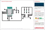
5. BLE2 click
™
board schematic
8. Support
7. Code examples
MikroElektronika offers free tech support
(www.mikroe.com/support) until the end
of the product’s lifetime, so if something
goes wrong, we’re ready and willing to help!
Once you have done all the necessary
preparations, it’s time to get your click
™
board
up and running. We have provided examples
for mikroC
™
, mikroBasic
™
and mikroPascal
™
compilers on our Libstock website. Just
download them and you are ready to start.
The RN4020 module aboard BLE2 click
™
incorporates a PCB antenna with a range
of at least 30m.
6. PCB antenna
C1
100nF
AN
RST
CS
SCK
MOSI
MISO
+3.3V
GND
PWM
INT
RX
TX
SCL
SDA
+5V
GND
MIKROBUS DEVICE CONN.
GND
AIO2
AIO1
AIO0
Tx
Rx
WAKE_SW
CMD/MLDP
G
N
D
PI
O
1
PI
O
2
PI
O
3
PI
O
4
PI
O
5
W
AK
E_
H
W
G
N
D
PIO
PIO6
PIO7
RSVD
RSVD
RSVD
VDD
GND
RN4020
M1
VCC_3.3V
E1
4.7uF
BT_UART_TX
BT_UART_RX
SWAKE
CMD/MLDP
CO
N
N
W
AK
E
LD1
R1
1K
LD2
R2
1K
CO
N
N
W
AK
E
VCC_3.3V
CONN
CMD/MLDP
BT_UART_TX
BT_UART_RX
R3
10K
SWAKE
SW
AK
E
.com


