8. Support
MikroElektronika offers
Free Tech Support
(www.mikroe.com/esupport)
until the
end of product lifetime, so if something goes
wrong, we are ready and willing to help!
7. Code Examples
.com
Once you have done all the necessary
preparations, it’s time to get your click
™
board up and running. We have provided
the examples for mikroC
™
, mikroBasic
™
and
mikroPascal
™
compilers on our
Libstock
website. Just download them and you are
ready to start.
VCC3.3
SSI0
SSI1
AN
RST
CS
SCK
MOSI
MISO
+3.3V
GND
PWM
INT
RX
TX
SCL
SDA
+5V
GND
C6
10pF
C10
10pF
C8
1nF
C4
10nF
C3
4.7uF
C7
1uF
C11
100nF
1
2
3
4
5
6
7
8
9
10
11
12
13
TX1
TX2
NC
NC
RX1
RX2
NC
GND_RX
ST
_R
0
N
C
N
C
U
R
X
VP
S
U
TX
14
15
16
17
18
19
20
21
22
23
24
25
26
27
28
29
30
31
32
C
S
M
IS
O
MOSI
SCK
SSI_0
SSI_1
ST_R1
GND
NC
NC
VP
S_
TX
G
N
D
_T
X
XO
U
T
XI
N
N
C
N
C
N
C
N
C
CR95HF
U8
CR95HF
R1
10K
R2
3K3
X1
27.12MHz
C5
150pF
C15
150pF
C13
220pF
C12
15pF
C9
N.M.
C14
N.M.
R27 330
R8 330
R4
N.M.
VCC3.3
C1
100nF
C2
10nF
VCC3.3
VCC3.3
VCC3.3
URX
UTX
SCK
MISO
MOSI
CS#
R3
100K
CS#
SCK
MISO
MOSI
J1
INT_O
TX
INT_O
INT_I
UTX
TX
J2
INT_I
RX
URX
RX
SSI1
SSI0
R5
3K3
VCC3.3
R6
3K3
VCC3.3
A
A
ANTENNA
FP1
FERRITE
R13
2K2
LD1
VCC3.3
R7 0
R10 0
R9
3K3
VCC3.3
B
B
MikroElektronika assumes no responsibility or liability for any errors or inaccuracies that may appear in the present document.
Specification and information contained in the present schematic are subject to change at any time without notice. Copyright © 2013 MikroElektronika. All rights reserved.
6. SMD jumpers
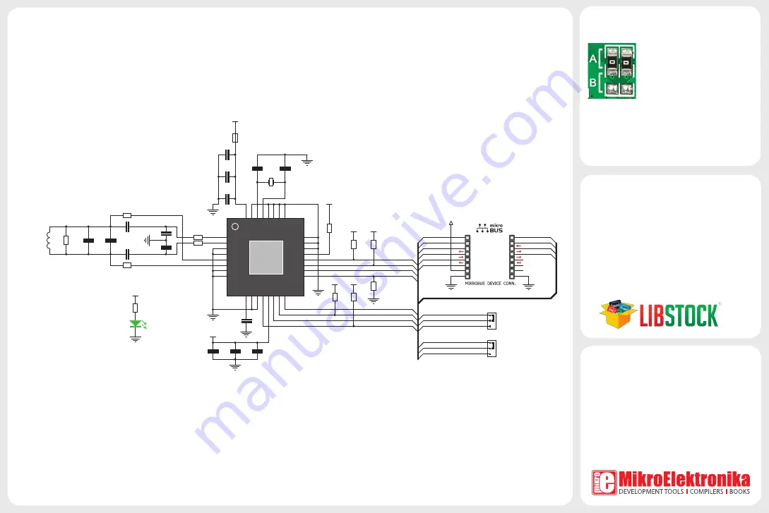
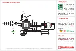
5. RFid click™ Board Schematic
Two SMD jumpers are
provided on the board. In
case you want to use UART
interface, it is necessary
to solder SMD jumpers in
B
position. Otherwise if you want to use
SPI interface, jumpers should be left in its
default position (
A
). In that case interrupt
pins (IN and OUT) are usable.


