*
内部资料
*
本文档中包含的信息涉及深圳迈瑞生物医疗电子股份有限公司秘密,均为内部保密信息,未经许可,不得外发。
Chapter4
Requirement and notes
1.1
Schematic and layout design guide
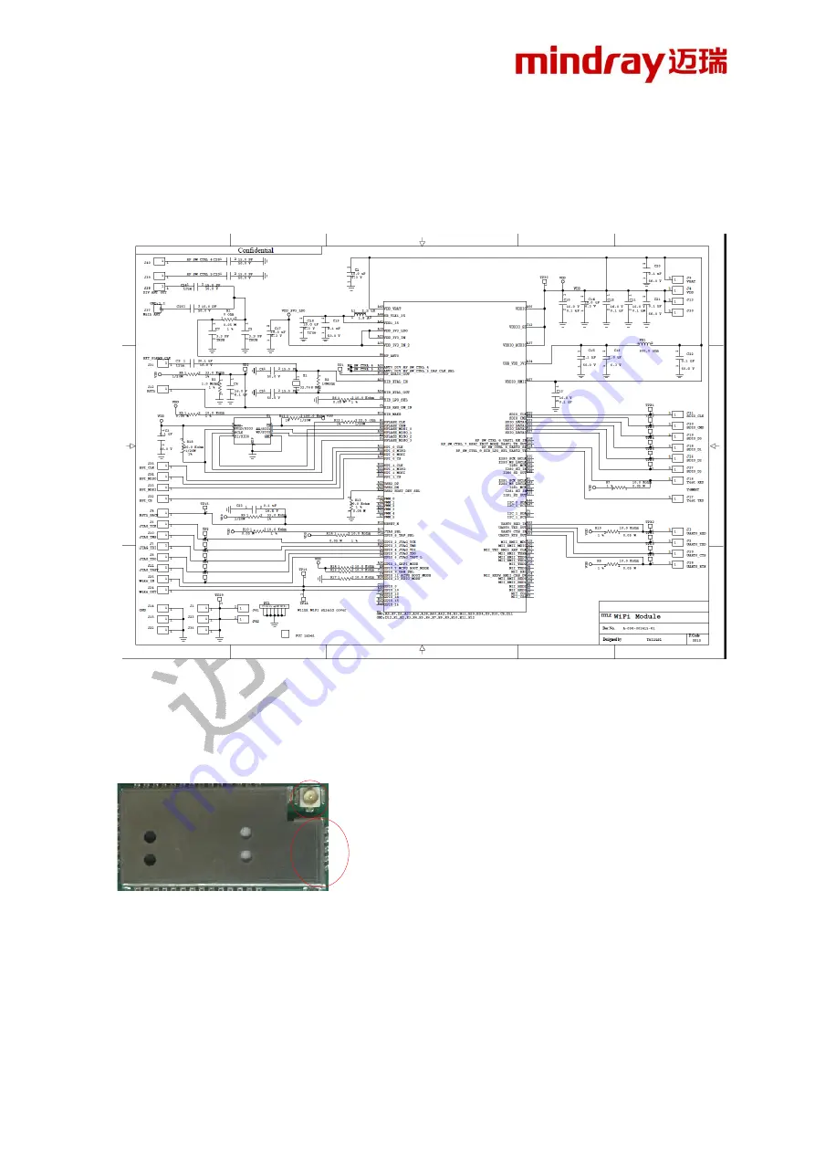
The schematic diagram of Wlink is as follows:
Precautions for carrier board layout:
1
,
The right half of Wlink is an analog circuit with antenna interface and diversity antenna circuit, as
shown in the figure below. Avoid running high-speed clock lines on the carrier board near the Wlink
analog circuit. Grounding is recommended.
2
,
There are test points on the bottom of Wlink, and the surface of the carrier board should avoid the risk
of short circuit caused by copper opening.
。


