background image

LCD MONITOR 15EX

LCD MONITOR 15EX

-

-

TA   MAINTENANCE

TA   MAINTENANCE

35

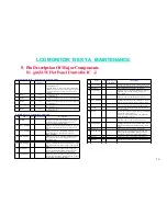
Unless otherwise stated, unused input pins must be tied to ground, and unused output pins left open.

Analog-to-Digital Converter. 

Pin Name  I/O 

Drive 

Current 

(@10pF) 

Description 

77  ADC_VDD2 


Digital power for ADC encoding logic. Must be 
bypassed with 0.1 uF capacitor to pin 78 
(ADC_GND2) 

78  ADC_GND2 


Digital GND for ADC encoding logic. Must be 
directly connected to the digital system ground 
plane. 

79  ADC_VDD1 


Digital power for ADC clocking circuit. Must be 
bypassed with 0.1 uF capacitor to pin 80 
(ACD_GND1) 

80  ADC_GND1 


Digital GND for ADC clocking circuit. Must be 
directly connected to the digital system ground 
plane. 

81  SUB_GNDA 


Dedicated pin for substrate guard ring that protects 
the ADC reference system. Must be directly 
connected to the analog system ground plane. 

82  ADC_GNDA 


Analog ground for ADC analog blocks that are 
shared by all three channels. Includes bandgap 
reference, master biasing and full scale adjust. Must 
be directly connected to analog system ground plane.

84  ADC_VDDA 


Analog power for ADC analog blocks that are shared 
by all three channels. Includes bandgap reference, 
master biasing and full scale adjust. Must be 
bypassed with 0.1 uF capacitor to pin 82 
(ADC_GNDA). 

83  Reserved 


For internal testing purpose only. Do not connect. 

85  ADC_BGNDA 


Analog ground for the blue channel. Must be directly 
connected to the analog system ground plane. 

88  ADC_BVDDA 


Analog power for the blue channel. Must be 
bypassed with 0.1 uF capacitor to pin 85 (BGNDA).

86  BLUE- 

In 


Negative analog input for the Blue channel. 

87  BLUE+ 

In 


Positive analog input for the Blue channel. 

89  ADC_GGNDA 


Analog ground for the green channel . Must be 
directly connected to the analog system ground 
plane. 

92  ADC_GVDDA 


Analog power for the green channe. Must be 
bypassed with 0.1 uF capacitor to pin 
89 (ADC_GGNDA). 

90  GREEN- 

In 


Negative analog input for the Green channel. 

91  GREEN+ 

In 


Positive analog input for the Green channel. 

93  ADC_RGNDA 


Analog ground for the red channel. Must be directly 
connected to the analog system ground plane. 


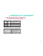
A n a lo g -to -D ig ita l  C o n v e r te r

P in

N a m e   I/O

D r iv e  

C u r r e n t

(@ 1 0 p F ) 

D e sc r ip tio n  

96

A D C _R V D D A


A nalog  pow er  for  the  red  channel.  M ust  be  bypassed 
w ith  0.1  uF  capacitor  to  pin  93  (A D C _R G N D A ). 

94

R E D - 

In 


N egative analog input for the R ed channel. 

95

R E D +  

In 


Positive analog input for the R ed channel. 


Host Interface (HIF) / External On-Screen Display 

Pin

Name I/O

Drive 

Current

(@10pF) 

Description 

98 HFS 

In 


Host Frame Sync. Frames the packet on the serial 
channel. 

103 HCLK 

In 


Clock signal input for the 3-wire serial 
communication. 

99 HDATA 

in/out

4 mA 

Data signal for the 3-wire serial communication 

100 RESETn 

In 


Resets the gmZAN1 chip to a known state when low. 

101 IRQ 

out

4 mA 

Interrupt request output 

115 OSD-HREF 

out

4 mA 

HSYNC output for an external OSD controller chip. 

116 OSD-VREF 

out

4 mA 

VSYNC output for an external OSD controller chip. 

117 OSD-Clk 

out

8 mA 

Clock output for an external OSD controller chip. 

118 OSD-Data0 

in 


Data input 0 from an external OSD controller. 

119 OSD-Data1 

in 


Data input 1 from an external OSD controller. 

120 OSD-Data2 

in 


Data input 2 from an external OSD controller. 

121 OSD-Data3 

in 


Data input 3 from an external OSD controller. 

122 OSD-FSW 

in 


External OSD window display enable. Displays data 
from external OSD con troller when high. 

123 MFB11 

in/out

8 mA 

Multi-Function Bus 11. One of twelve multi-function 
signals MFB[11:0]. 

124 MFB10 

in/out

8 mA 

Multi-Function Bus 10. One of twelve multi-function 
signals MFB[11:0]. 

102 MFB9 

in/out

8 mA 

Multi-Function Bus 9. One of twelve multi-function 
signals MFB[11:0]. 
Also used as HDATA3 in a 4-bit host interface 
configuration. 

104 MFB8 

in/out

8 mA 

Multi-Function Bus 8. One of twelve multi-function 
signals MFB[11:0]. 
Also used as HDATA2 in a 4-bit host interface 
configuration. 

105 MFB7 

in/out

8 mA 

Multi-Function Bus 7. One of twelve multi-function 
signals MFB[11:0]. 
Also used as HDATA1 in a 4-bit host interface 
configuration. 

5.  

5.  

Pin Description Of Major Components

Pin Description Of Major Components

5.1  gmZAN1 Flat Panel Controller IC  

5.1  gmZAN1 Flat Panel Controller IC  

-

-

1

1

Summary of Contents for 15EX-TA

Page 1: ...OLOGY DEPARTMENT TSSC TESTING TECHNOLOGY DEPARTMENT TSSC BY BY Richard Wang Richard Wang JUN 2001 JUN 2001 SERVICE MANUAL TROUBLESHOOTING GUIDE FOR SERVICE MANUAL TROUBLESHOOTING GUIDE FOR SERVICE MAN...

Page 2: ...ion Location Of Connectors Jumpers 3 1 15EX TA Interface Board 3 2 Power Jack Board 3 3 3 Invertor Board 3 4 Phone Jack Board 3 5 Key Switch Board 3 6 Relation Of All Components 4 4 Definition Locatio...

Page 3: ...Display Abnormal 7 3 OSD Function Or Display Abnormal 7 4 No Back light 7 5 PC Can t Detect LCD Monitor Type 7 6 LCD Monitor Audio Function Abnormal 8 Spare Parts List 8 Spare Parts List 9 System Exp...

Page 4: ...768 color LCD monitor which uses 15 high contrast TFT LCD panel This monitor supplies user with following features On screen display adjustment function Multi sync process DPMS power saving function...

Page 5: ...MONITOR 15EX LCD MONITOR 15EX TA MAINTENANCE TA MAINTENANCE 4 1 2 MAIN CHARACTERISTICS 1 2 1 LCD PANEL LCD panel 15 color TFT LCD Model no 1 HYUNDAI HT15X11 200 2 CHI MEI M150X1 01 3 HANNSTAR HSD150MX...

Page 6: ...dth Input video voltage range 0 6 0 95 Vp p typ 0 7 Vp p Impedance 75 5 50 pF max 1 2 4 SCAN FREQUENCY Horizontal frequency 24 8 60 kHz Vertical frequency 56 75 Hz Polarity positive or negative 3V 5V...

Page 7: ...AL CONTROLLER OUTLET LCD control key MENU SELECT BRIGHTNESS POWER 1 2 10 AC INPUT POWER Max 264 Vac 50 Hz Min 90 Vac 60 Hz Normal 100 240 Vac 60 50 Hz 1 2 11 POWER SAVING FUNCTION INDICATOR COMPLY WIT...

Page 8: ...LCD MONITOR 15EX LCD MONITOR 15EX TA MAINTENANCE TA MAINTENANCE 7 1 2 13 COMPATIBLE TIMING CHART...

Page 9: ...LCD MONITOR 15EX LCD MONITOR 15EX TA MAINTENANCE TA MAINTENANCE 8 1 2 14 MAIN OSD MENU...

Page 10: ...LCD MONITOR 15EX LCD MONITOR 15EX TA MAINTENANCE TA MAINTENANCE 9...

Page 11: ...y Operation Pushing Menu key the OSD window will pop out The default value will focus on the first icon Keep pushing Menu key the highlight will go to next item The sequence is DISP ADJUSTMENT menu WH...

Page 12: ...STING NO SIGNAL SCREEN Message Displayed Position Secret Key Operation AGING Menu Select Right and Power ON VERSION Menu Left Right and Power ON Version Displayed Position MODEL NAME T15EX VERSION R00...

Page 13: ...the FACTORY USED ONLY menu Press Select Key to select the item Press Menu Key to execute the function Press Power Key to exit This menu will set the auto backlight rank to 0 and turn on the auto mode...

Page 14: ...run this procedure again Press select key will go to next item MIN 0 LUX item This will set the minimum value for program HEX Number Put the 0Lux light to sensor board and press menu key to start set...

Page 15: ...LCD MONITOR 15EX LCD MONITOR 15EX TA MAINTENANCE TA MAINTENANCE 14 Relation with LUX from Rank 0 to Rank 4 Note 0 31 is LIGHT LEVEL...

Page 16: ...LCD MONITOR 15EX LCD MONITOR 15EX TA MAINTENANCE TA MAINTENANCE 15 1 3 HARDWARE SYSTEM BLOCK DIAGRAM...

Page 17: ...API 208 98010M Note 1 68 min at full load 115Vac 60Hz Note 2 No max limits but in hot start shall no damage Fuse could not open Note 1 The ripple and regulation shall be maintained in the SPEC for all...

Page 18: ...NITOR 15EX TA MAINTENANCE TA MAINTENANCE 17 2 2 System Assembly Disassembly System Assembly Disassembly 2 1 System View 2 1 1 Front View Menu Button Select Button Buttons Auto Adjustment Button Power...

Page 19: ...LCD MONITOR 15EX LCD MONITOR 15EX TA MAINTENANCE TA MAINTENANCE 18 2 2 System Assembly Disassembly System Assembly Disassembly 2 1 2 Side View Microphone Input Connector Headphone Output Connector...

Page 20: ...LCD MONITOR 15EX LCD MONITOR 15EX TA MAINTENANCE TA MAINTENANCE 19 2 2 System Assembly Disassembly System Assembly Disassembly 2 1 3 Rear View VESA Mounting Holes Power Connector Signal Cable Latch...

Page 21: ...component for disassembly reassembly and show corresponding illustrations CAUTION Before you start to install replace these modules 1 Turn off the power button on the rear panel of the monitor 2 Disc...

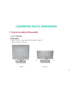
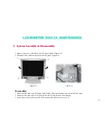
Page 22: ...INTENANCE TA MAINTENANCE 21 2 2 System Assembly Disassembly System Assembly Disassembly 2 2 1 LCD Panel Disassembly 1 Remove the screw cover on the rear side of the monitor Figure 2 1 2 Remove three s...

Page 23: ...NTENANCE 22 2 2 System Assembly Disassembly System Assembly Disassembly 3 To detach the LCD frame first lift the lower edge and then separate it from the housing Figure 2 3 4 Disconnect the cable conn...

Page 24: ...htly Figure 2 5 6 Disconnect three cables connected to the LCD panel Figure 2 6 Figure 2 5 Figure 2 6 Reassembly 1 Reconnect the cables to the LCD panel then fit the LCD panel into place and secure wi...

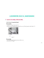
Page 25: ...embly Disassembly 2 2 2 Power Connector Board Disassembly 1 Detach the LCD panel See section 2 2 1 2 Remove one screw locking the connector board then you can lift up the connector board Figure 2 7 Fi...

Page 26: ...Disassembly 2 2 3 Signal Cable Disassembly 1 Detach the LCD panel See section 2 2 1 2 Remove one screw locking the cover and lift it up then you can pull out the signal cable Figure 2 8 Figure 2 8 Re...

Page 27: ...ove the screw cover on the rear side of the monitor 2 Remove four screws locking the base unit and then lift the LCD panel up see figure 2 9 Figure 2 9 Reassembly 1 Replace the base unit and secure wi...

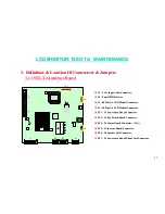
Page 28: ...1 To Power Jack Board Connector JP1 To Power Jack Board Connector JP2 To Key Switch Board Connector JP2 To Key Switch Board Connector JP4 To Sensor Board Connector N A JP4 To Sensor Board Connector N...

Page 29: ...Phone Jack Connector J1 Audio In Phone Jack Connector J2 To Phone Jack Board Connector J2 To Phone Jack Board Connector J3 MIC_OUT Phone Jack Connector J3 MIC_OUT Phone Jack Connector JP1 To Interfac...

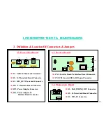
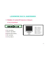
Page 30: ...ctors Jumpers 3 5 Key Switch Board SW1 Power Button SW1 Power Button SW2 SW5 Adjust Button SW2 SW5 Adjust Button SW3 SW4 OSD Select Button SW3 SW4 OSD Select Button SW6 Auto Button SW6 Auto Button D1...

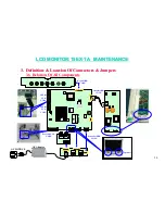
Page 31: ...ANCE 30 3 3 Definition Location Of Connectors Jumpers Definition Location Of Connectors Jumpers AC SOURCE AC Adapter Key SW BD CONN Power Jack BD CONN External VGA CONN 40 Pins LCD CONN 20 Pins LCD CO...

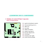
Page 32: ...Trigger Inverters U2 74F14 Hex Schmitt Trigger Inverters U3 M52347 N A U3 M52347 N A U5 24C21 EDID U5 24C21 EDID U6 HIP6013 Switch Regulator U6 HIP6013 Switch Regulator U7 EZ1084CT Linear Regulator U7...

Page 33: ...ltering Sync On Green SOG and an enhanced OSD Features Features Fully integrated 135MHz 8 Fully integrated 135MHz 8 bit triple bit triple ADC PLL and pre ADC PLL and pre amplifier amplifier gmZ2 scali...

Page 34: ...and image positioning Phase and image positioning Input format detection Input format detection Operating Modes Operating Modes Bypass mode with no filtering Bypass mode with no filtering Multiple zoo...

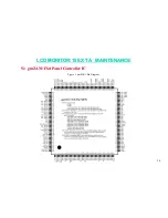
Page 35: ...LCD MONITOR 15EX LCD MONITOR 15EX TA MAINTENANCE TA MAINTENANCE 34 Figure 1 gmZAN1 Pin Diagram 5 1 5 1 gmZAN1 Flat Panel Controller IC gmZAN1 Flat Panel Controller IC...

Page 36: ...channel 93 ADC_RGNDA Analog ground for the red channel Must be directly connected to the analog system ground plane Analog to Digital Converter Pin Nam e I O Drive Current 10pF Description 96 ADC_RVD...

Page 37: ...n DDS Must be directly connected to the analog system ground plane 133 SUB_SGNDA Dedicated pin for the substrate guard ring that protects the Source DDS Must be directly connected to the analog system...

Page 38: ...out 2 mA 20 mA EB3 EB1 B3 B1 54 PD12 out 2 mA 20 mA EB2 EB0 B2 B0 55 PD11 out 2 mA 20 mA EG7 EG5 G7 G5 56 PD10 out 2 mA 20 mA EG6 EG4 G6 G4 Pin Name I O Drive Current 10pF Description 2pxl clk 2pxl c...

Page 39: ...r automatic PCB assembly testing 160 SCAN_OU T2 out Scan output 2 used for automatic PCB assembly testing 153 Reserved 154 Reserved VDD VSS for Core Circuitry Host Interface and Panel Memory Interface...

Page 40: ...onitor power in 15EX INTERFACE BOARD Interface Board Receive PC VGA signals transfer to LCD signals control inverter BD backlight up down Power Jack Board AC power Transfer to DC and provide system po...

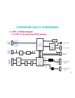
Page 41: ...Diagram TA Block Diagram 6 6 2 15EX 2 15EX TA Interface Board Block diagram TA Interface Board Block diagram J1 External VGA Analog RGB U1 gmZAN1 Flat Panel Monitor Controller IC ESD Protective Circu...

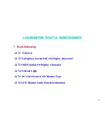
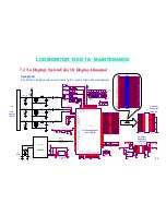
Page 42: ...No Display System Fail Or Display Abnormal 7 3 OSD Function Or Display Abnormal 7 3 OSD Function Or Display Abnormal 7 4 No Back Light 7 4 No Back Light 7 5 PC Can 7 5 PC Can t Detect LCD Monitor Typ...

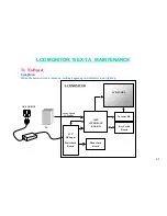
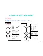
Page 43: ...ing happens power indica When the power switch is turned on nothing happens power indicator is not light up tor is not light up 7 1 7 1 No Power No Power PC 12V DC Input Power Jack Board Key Switch Bo...

Page 44: ...70 165 0603 1 1 2 U7 EZ1084CT 3 1 2 4 VIN GND VOUT0 VOUT1 C77 10uF 16V CPWX4 3 1 2 C78 10uF 16V CPWX4 3 1 2 R67 100 0603 1 1 2 D9 1N4148 MLL34B A K R111 10K 0603 1 2 C73 0 1uF 1 2 Q14 2sc1623 B E C R1...

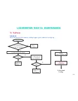
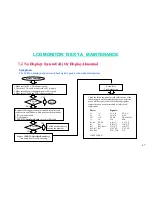
Page 45: ...ht up ator is not light up Board Board level level Troubleshooting Troubleshooting Replace Replace 15EX TA Interface Board No power No power Connect AC adaptor Replace the faulty AC Adaptor Power Powe...

Page 46: ...No Check following parts and signals PARTS SIGNAL D14 R117 U14 R120 R112 R115 R116 R119 C157 C158 VDD_12 5VP Yes End Check following parts and signals PARTS SIGNAL Q4 Q5 D12 B22 R72 R76 12VIN VDD_12...

Page 47: ...0 1uF C8 22uF 16V 10V C9 0 1uF C11 0 1uF C12 0 1uF B14 120z 100M 1 2 B17 120z 100M 1 2 B16 120z 100M 1 2 B18 120z 100M 1 2 C26 0 1uF C14 0 1uF C165 0 1uF B83 220Z 100M R11 100 C46 0 01uF R12 100 R35...

Page 48: ...cture OK YES NO Replace 15EX TA Interface Board or go into board level Trouble shooting To find out which part is causing the problem 1 Make sure the PC VGA adapter is good 2 Check the VGA cable is co...

Page 49: ...PARAMETER EEPROM U11 M6759 21 20MHz C97 22P Y2 C96 22P 20 R53 HDATA 0 3 U1 gmZAN1 J3 To Panel Connector 40 Pins J4 To Panel Connector 20 Pins JP5 To Inverter Connector 12VIN GND GND GND 5V GND 5V BRI...

Page 50: ...le shooting Replace Key SW BD and To find out which part is causing the problem OSD function OK NO YES Try another known good Key SW BD 1 Make sure that Key SW BD and 15EX TA Interface Board is connec...

Page 51: ...146 0 1uF C145 100uF 25V CPWX8 3 B78 500z 100M PH_5P 1 2 3 4 5 TO INVERTER 12V GND GND BRT_RANGE ON OFF 21 20MHz C97 22P Y2 C96 22P 20 R53 HDATA 0 3 U1 gmZAN1 J3 To Panel Connector 40 Pins J4 To Panel...

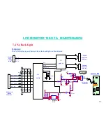
Page 52: ...t after each replacement until find out which part caused the problem 1 LCD module 2 Inverter BD 3 15EX TA Interface Board to inverter BD cable Check the following parts for cold solder or one of the...

Page 53: ...t Detect The LCD Monitor Type t Detect The LCD Monitor Type GND VCC_FROM_PC GND VCC_FROM_PC DDC_SCL VSYNC DDC_SDA R57 100 R56 100 R58 100 R55 47K R54 47K C64 0 1uF C66 47P U5 24C21 8 1 2 3 4 7 6 5 VC...

Page 54: ...ble Is it OK NO YES END Replace PC to monitor cable Check the following parts for cold solder or one of the following parts on the mother board may be defective use an oscilloscope to check the follow...

Page 55: ..._PHONE_R EAR_PHONE_R AUDIO_IN_L AUDIO_IN_R GND GND TO DC JACK BD TO SPEAKER UNIT SPK_R SPK_R SPK_L SPK_L L R 12VIN VDD_12 AUDIO_PWR L2 500Z 100M R124 47K MMBT3906L U15 TPS1100D 1 2 3 4 5 6 7 8 SOURCE1...

Page 56: ...VGA adapter is good 2 Check the Audio Input Signal is working properly 3 Make sure all cable and PCB connect properly Replace 15EX TA Interface Board or go into board level Trouble shooting 7 6 7 6 L...

Page 57: ...SMT C18 272005102401 CAP 1000P CR 50V 10 0805 X7R 627207510031 CAP 10P 50V 5 0603 NPO SMT C122 C17 C30 C41 Part Number Description Location s 272075150301 CAP 15P CR 50V 5 0603 NPO SMT C49 2720031057...

Page 58: ...R 15AX 648115130001 F W ASSY 2421 DDC SO8 15EX HANN STAR 648115130002 F W ASSY MX10FMAXD PLCC44 15EX HSD Part Number Description Location s 627300130010 FERRITE CHIP 120OHM 100MHZ 1608 10 S B1 B2 B3 B...

Page 59: ...CD BRACKET R HANNSTAR 2 15EX 641300020057 LCD HSD150MX42 A 15 TFT HANNSTAR 634615080009 LED HOLDER LED 9 1511A 50UX R8 634615120002 LED HOLDER S W BD LED 5 3 50AX D1 Part Number Description Location s...

Page 60: ...71071165011 RES 165 1 16W 1 0603 SMT R70 271002102301 RES 1K 1 10W 5 0805 SMT R69 627107110231 RES 1K 1 16W 5 0603 SMT R103 R105 R112 R128 R7 Part Number Description Location s 627107110531 RES 1M 1 1...

Page 61: ...TRANS HUF75307 N MOSFET TO252 SMT Q3 288203904002 TRANS MMBT3904 40V 200mA SOT23 MUSTAN Q1 288203904010 TRANS MMBT3904L NPN Tr35NS TO236AB Q10 Q11 Q12 Q13 Q14 Q 288203906018 TRANS MMBT3906L PNP Tr35NS...

Page 62: ......

Page 63: ...m 10P to 15P EMI 8 Add C17 C29 C36 15P EMI 9 Add C149 1000P EMI 6 Add B69 B70 B71 B72 B73 120z 100MHz EMI 10 Change B65 B66 B67 from 220Z 100MHz to 0 ohm 1206 EMI 11 Change R25 R40 from 510 ohm to 100...

Page 64: ...C_GVDDA ADC_RGNDA RED RED ADC_RVDDA N C HFS HDATA RESETn IRQ MFB9 HCLK CVDD4 CVSS4 OSD_HREF OSD_VREF OSD_CLK OSD_DATA0 OSD_DATA1 OSD_DATA2 OSD_DATA3 OSD_FSW MFB11 MFB10 DVDD DVSS DAC_DGNDA DAC_DVDDA P...

Page 65: ...00M 3216 1 2 Q10 MMBT3904L R65 499 1 2 R62 2 94K 1 2 R63 40 2K 0805 1 2 Q7 MMBT3904L GND OUT VCC U9 KIA7042 3 1 2 U13 KIA7045 E B C RSTN VCC GND R80 470 J2 3PX1 1 MA GOLD 1 2 3 1 2 3 JP4 HEADER_4 1 2...

Page 66: ...26 27 28 29 30 31 32 33 34 35 36 37 38 39 40 MTG3 ID3 2 OD8 0 4 5 6 7 9 10 1 2 3 8 11 12 MTG2 ID3 2 OD8 0 4 5 6 7 9 10 1 2 3 8 11 12 B56 120z 100M 1 2 B54 120z 100M 1 2 B52 120z 100M 1 2 B64 120z 100M...

Page 67: ...SPK_R EAR_PHONE_L EAR_PHONE_R SPK_R AUDIO_PWM AUDIO_PWR 5V AUDIO_GND AUDIO_GND AUDIO_GND AUDIO_GND GND AUDIO_GND AUDIO_GND GND AUDIO_GND 12VIN VDD_12 JP7 8HEADER 1 2 3 4 5 6 7 8 R108 10K L2 500Z 100M...

Page 68: ...KEY_UP KEY_DOWN HOT_KEY SOFT_PWR LED_AMBER LED_GREEN GND TO INTERFACE BD 15EX TA KEY SW BD 01 B 1 1 Title Size Document Number Rev Date Sheet of KEY_MENU KEY_SELECT KEY_UP KEY_DOWN HOT_KEY SOFT_PWR LE...

Page 69: ...HONE_R EAR_PHONE_L EAR_PHONE_L PCB 630015130006 PCBA 640015130006 TO POWER JACK BD 15EX TA PHONE JACK BD 01 A 1 1 Title Size Document Number Rev Date Sheet of MIC_IN_R EAR_PHONE_L GND EAR_PHONE_R MIC_...

Page 70: ...E_L EAR_PHONE_L EAR_PHONE_R TO INTERFACE BD TO PHONE JACK BD 12V 12V NC GND GND 15EX TA POWER JACK BD 01 B 1 1 Title Size Document Number Rev Date Sheet of MIC_OUT_R AUDIO_IN_L AUDIO_IN_R EAR_PHONE_L...

Page 71: ...GND GND GND R12 LS1001 NC FD4 FIDUCIAL MARK 1 FD3 FIDUCIAL MARK 1 FD2 FIDUCIAL MARK 1 FD1 FIDUCIAL MARK 1 Q1 MMBT3904L C2 0 1uF C1 0 047uF C4 0 1uF MTG3 ID3 2 OD8 0 4 5 6 7 9 10 1 2 3 8 11 12 MTG2 ID3...

Page 72: ...TOR 15EX LCD MONITOR 15EX TA MAINTENANCE TA MAINTENANCE 61 REFERENCE MATERIAL 15EX TA ENGINEERING SPECIFICATION Jeff Lee Mitac gmZAN1 DATA SHEET Genesis Microchip Co THE HM15EX TA PRODUCT SPEC Jeff Le...

Page 73: ...C INTERNATIONAL CORP Address 4F NO 18 PU DING ROAD HSINCHU TAIWAN R O C TEL 886 3 5645850 Fax 886 3 5781245 First Edition Jun 2001 E mail Jesse Jan mic com tw SERVICE MANUAL TROUBLESHOOTING GUIDE FOR...

Reviews: