LCD MONITOR 15EX
LCD MONITOR 15EX
-
-
TA MAINTENANCE
TA MAINTENANCE
36
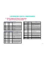
Host Interface (HIF) / External On-Screen Display
Pin Name I/O
Drive
Current
(@10pF)
Description
107 MFB5
in/out
8 mA
Multi-Function Bus 5. One of twelve multi-function
signals MFB[11:0].
Internally pulled up. When externally pulled down
(sampled at reset) the chip uses an external crystal
resonator across pins 141 and 142, instead of an
oscillator.
109 MFB4
in/out
8 mA
Multi-Function Bus 4. One of twelve multi-function
signals MFB[11:0].
110 MFB3
in/out
8 mA
Multi-Function Bus 3. One of twelve multi-function
signals MFB[11:0].
111 MFB2
in/out
8 mA
Multi-Function Bus 2. One of twelve multi-function
signals MFB[11:0].
112 MFB1
in/out
8 mA
Multi-Function Bus 1. One of twelve multi-function
signals MFB[11:0].
113 MFB0
in/out
8 mA
Multi-Function Bus 0. One of twelve multi-function
signals MFB[11:0].
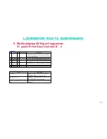
Clock Recovery / Time Base Conversion
Pin Name I/O
Drive
Current
(@10pF)
Description
125 DVDD
Digital power for Destination DDS (direct digital
synthesizer). Must be bypassed with a 0.1 uF
capacitor to digital ground plane.
127 DAC_DGNDA
Analog ground for Destination DDS DAC. Must be
directly connected to the analog system ground
plane.
128 DAC_DVDDA
Analog power for Destination DDS DAC. Must be
bypassed with a 0.1 uF capacitor to pin 127
(DAC_DGNDA)
129 PLL_DVDDA
Analog power for the Destination DDS PLL. Must
be bypassed with a 0.1 uF capacitor to pin 131
(PLL_DGNDA)
130 Reserved
For testing purposes only. Do not connect.
131 PLL_DGNDA
Analog ground for the Destination DDS PLL. Must
be directly connected to the analog system ground
plane.
132 SUB_DGNDA
Dedicated pin for the substrate guard ring that
protects the Destination DDS. Must be directly
connected to the analog system ground plane.
133 SUB_SGNDA
Dedicated pin for the substrate guard ring that
protects the Source DDS. Must be directly connected
to the analog system ground plane.
Pin
Name I/O
Drive
Current
(@10pF)
Description
134 PLL_SGNDA
Analog ground for the Source DDS PLL. Must be
directly connected to the analog system ground.
135 Reserved
For testing purposes only. Do not connect.
136 PLL_SVDDA
Analog power for the Source DDS PLL. Must be
bypassed with a 0.1 uF capacitor to pin 134
(PLL_SGNDA)
137 DAC_SVDDA
Analog power for the Source DDS DAC. Must be
bypassed with a 0.1 uF capacitor to pin 138
(DAC_SGNDA)
138 DAC_SGNDA
Analog ground for the Source DDS DAC. Must be
directly connected to the analog system ground.
139 SVDD
Digital power for the Source DDS. Must be bypassed
with a 0.1 uF capacitor to digital ground plane.
141 TCLK
in
Reference clock (TCLK) input from the 50 Mhz
crystal oscillator.
142 XTAL
out
If using an external oscillator, leave this pin floating.
If using an external crystal,
connect crystal between TCLK (141) and XTAL
(142). See MFB5 (pin 107).
143 PLL_RVDDA
Analog power for the Reference DDS PLL. Must be
bypassed with a 0.1 uF capacitor to pin 144
(PLL_RGNDA)
144 PLL_RGNDA
Analog ground for the Reference DDS PLL. Must be
directly connected to the analog system ground
plane.
145 Reserved
For testing purposes only. Do not connect.
146 SUB_RGNDA
Dedicated pin for the substrate guard ring that
protects the Reference DDS. Must be directly
connected to the analog system ground plane.
148 VSYNC
in
CRT Vsync input. TTL Schmitt trigger input.
149 SYN_VDD
Digital power for CRT Sync input
150 HSYNC/
CSYNC
in
CRT Hsync or CRT composite sync input. TTL
Schmitt trigger input.
5.
5.
Pin Description Of Major Components
Pin Description Of Major Components
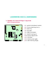
5.1 gmZAN1 Flat Panel Controller IC
5.1 gmZAN1 Flat Panel Controller IC
-
-
2
2


