71
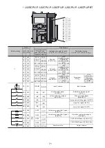
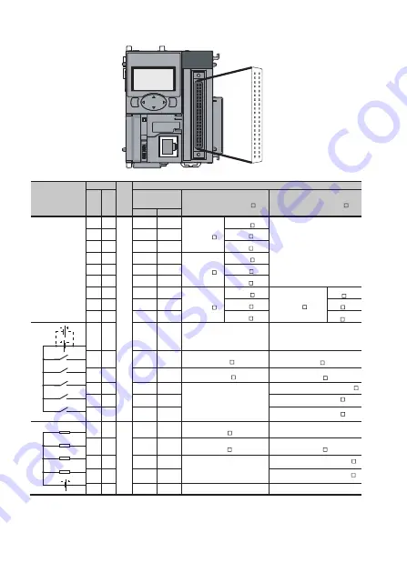
• L02SCPU-P, L02CPU-P, L06CPU-P, L26CPU-P, L26CPU-PBT
B20
B19
B18
B17
B16
B15
B14
B13
B12
B11
B10
B09
B08
B07
B06
B05
B04
B03
B02
B01
A20
A19
A18
A17
A16
A15
A14
A13
A12
A11
A10
A09
A08
A07
A06
A05
A04
A03
A02
A01
B20
A20
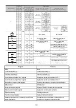
IN0-24V
IN2-24V
B19
A19
IN0-DIFF IN2-DIFF
B18
A18
IN0-COM IN2-COM
B17
A17
IN1-24V
IN3-24V
B16
A16
IN1-DIFF IN3-DIFF
B15
A15
IN1-COM IN3-COM
B14
A14
IN4-24V
IN5-24V
B13
A13
IN4-DIFF IN5-DIFF
B12
A12
IN4-COM IN5-COM
B11
A11
INCOM
INCOM
B10
A10
IN6
IN7
B09
A09
IN8
IN9
B08
A08
INA
INB
B07
A07
INC
IND
B06
A06
INE
INF
B05
A05
OUT0
OUT1
B04
A04
OUT2
OUT3
B03
A03
OUT4
OUT5
B02
A02
OUT6
OUT7
B01
A01
OUT24V OUT24V
Output common
Input
Coincidence output No.2 signal
(EQU 2)
Coincidence output No.1 signal
(EQU 1)
+24V
(PULSE Z -24V)
CW/PULSE/Phase A (PULSE F )
CCW/SIGN/Phase B (PULSE R )
*1
-
-
Deviation counter clear signal
(CLEAR )
-
Zero signal
(PG0 )
Input common
-
Latch counter input signal
(LATCH )
Out
put
Output common
Input common
Upper limit signal (FLS )
External command signal
(CHG )
Drive unit ready signal
(READY )
Near-point watchdog signal (DOG )
+24V
(PULSE A -24V)
Differential
(PULSE A -DIFF)
COM
(PULSE A -COM)
+24V
(PULSE B -24V)
Differential
(PULSE B -DIFF)
COM
(PULSE B -COM)
Lower limit signal (RLS )
+24V
(PG0 -24V)
Differential
(PG0 -DIFF)
COM
(PG0 -COM)
Differential
(PULSE Z -DIFF)
COM
(PULSE Z -COM)
Function input signal
(FUNC )
External wiring
Pin No.
CH1
(Axis 1)
CH2
(Axis 2)
I/O
General-purpose I/O,
Interrupt, and
Pulse catch functions
Row B
Row A
Signal name
Load
Load
Load
Load
High-speed counter function
(1 (CH1) or 2 (CH2) is in .)
Positioning function
(1 (Axis 1) or 2 (Axis 2) is in .)
Phase A
(PULSE A )
Phase B
(PULSE B )
Phase Z
(PULSE Z )
Summary of Contents for 13J240
Page 76: ...75 Memo ...
Page 79: ......

