1
8
P
C
K
N
-O
IL
73
8
Undervoltage CA phase Ind.
Undervoltage AB phase Ind.
Undervoltage BC phase Ind.
Overvoltage CA phase Ind.
Overvoltage AB phase Ind.
Overvoltage BC phase Ind.
U >
Setting
switches
A/D
Numerical display
A-07
V
AB
A-08
S/H
Filter
Trip
X5
X4
X3
X2
X1
X0
Communication indication
Unit indication
Trip indication
Power circuit
monitoring
A-01
AC/DC
DC/DC
Power
source
Auxiliary
power supply
A-03
+
Y
X5
B-19
B-20
X4
B-17
B-18
Trip contacts
Programmable output
B-07
B-08
X0
B-09
B-10
X1
B-11
B-12
X2
B-13
B-14
X3
Signaling
Self-diagnosis output
Y
Self-diagnosis output
B-05
B-06
Serial
communication
bus
DA
B-01
DB
B-02
DG
B-03
SLD
B-04
E
A-02
Run indication
Self-diagnosis
(Except comm. card)
Communication card
Self-diagnosis (only comm. card)
Reception circuit
Transmission circuit
MPX
CP
U
Overvoltage
element
A-09
V
BC
A-10
S/H
Filter
A-11
V
CA
A-12
S/H
Filter
UV Test indication
Undervoltage
element
U <
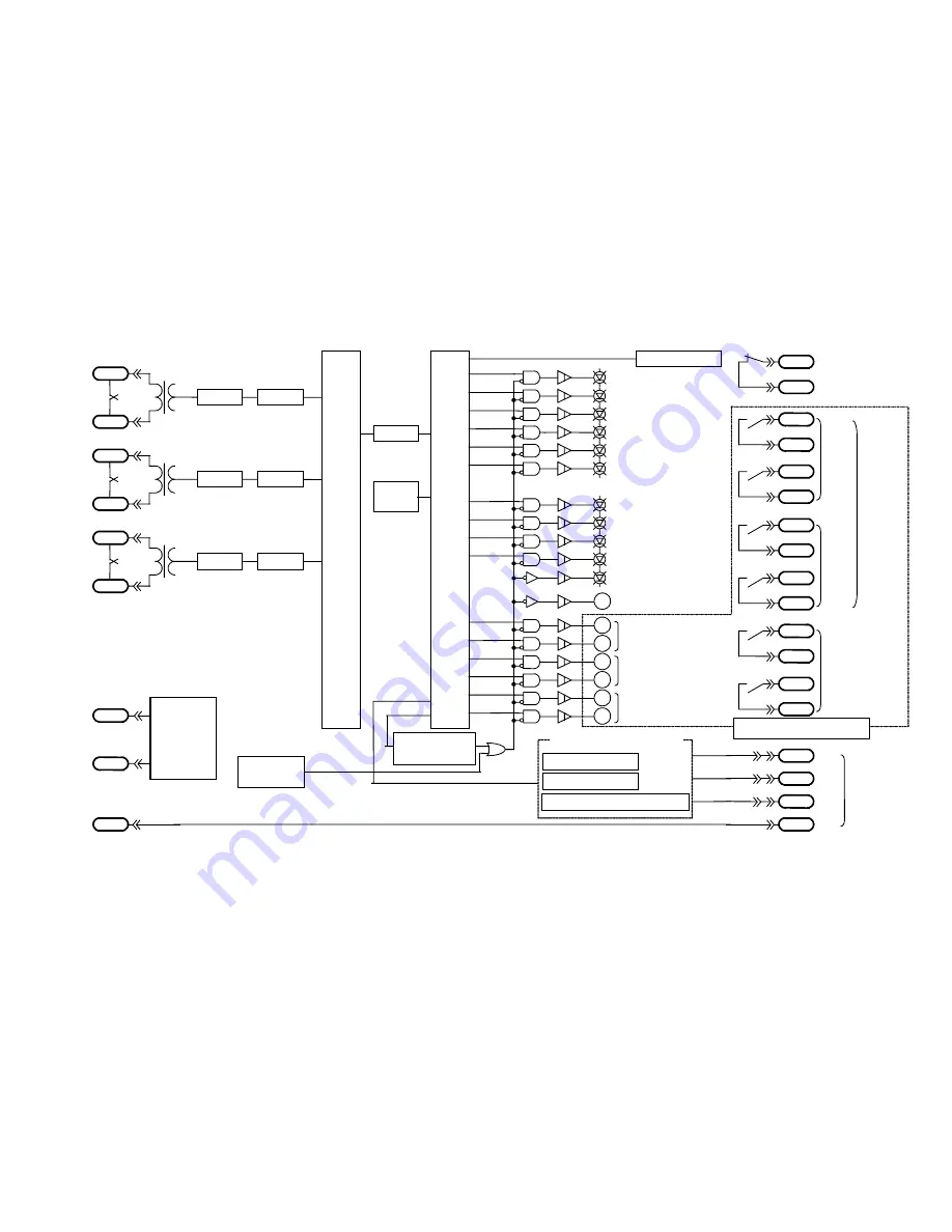
Figure 5.1 Internal block diagram of Type CBV2-A01D1 relay


