8. Connections of I/O Interface
8.3 Connecting with Scan I/O Card
119
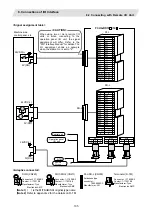
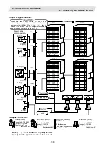
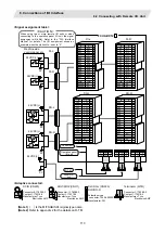
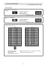
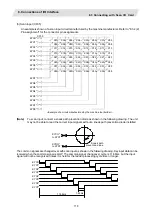
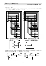
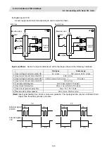
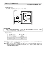
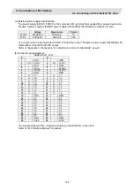
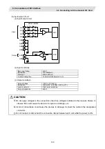
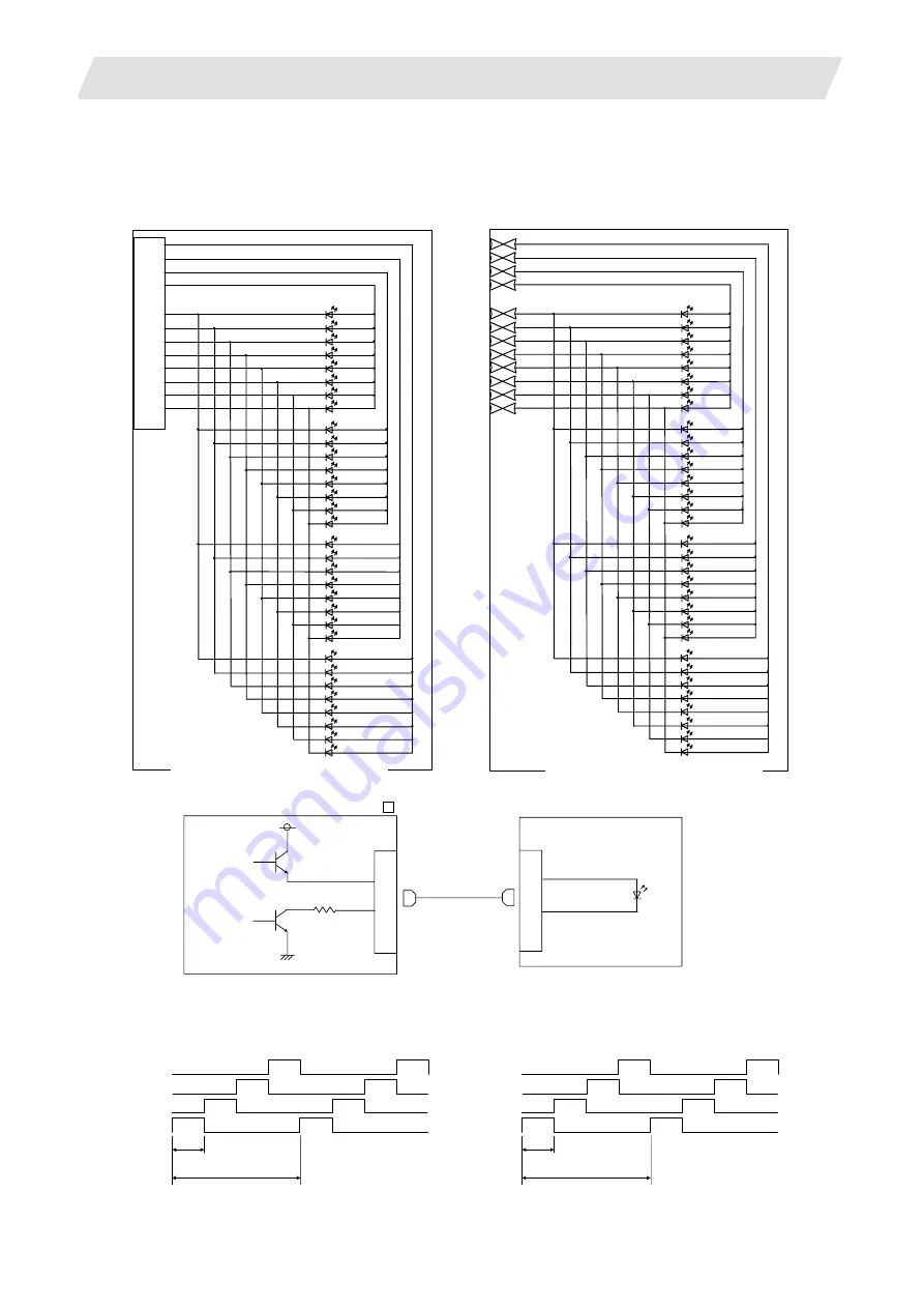
(4) Scan output (CF35)
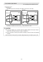
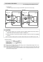
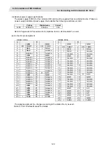
An example is shown of a scan output circuit manufactured by the machine manufacturer. Refer to "8.3.2
(2) Pin assignment" for the connector pin assignments.
CF35
LC3A
LC2A
LC1A
LC0A
LD0A*
LD1A*
LD2A*
LD3A*
LD4A*
LD5A*
LD6A*
LD7A*
Y00
Y01
Y02
Y03
Y04
Y05
Y06
Y07
Y08
Y09
Y0A
Y0B
Y0C
Y0D
Y0E
Y0F
Y10
Y11
Y12
Y13
Y14
Y15
Y16
Y17
Y18
Y19
Y1A
Y1B
Y1C
Y1D
Y1E
Y1F
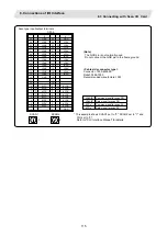
CF35
LC3B
LC2B
LC1B
LC0B
LD0B*
LD1B*
LD2B*
LD3B*
LD4B*
LD5B*
LD6B*
LD7B*
Y20
Y21
Y22
Y23
Y24
Y25
Y26
Y27
Y28
Y29
Y2A
Y2B
Y2C
Y2D
Y2E
Y2F
Y30
Y31
Y32
Y33
Y34
Y35
Y36
Y37
Y38
Y39
Y3A
Y3B
Y3C
Y3D
Y3E
Y3F
<Example of a circuit manufacturerd
by the machine tool builder>
<Example of a circuit manufacturerd
by the machine tool builder>
Output circuit
<Manufactured by the machine tool builder>
CF35
5V
LCnA/B
LDnA/B*
330
Ω
0V(RG)
HR3 7
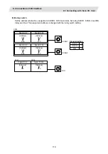
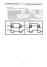
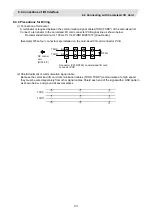
The common signals are changed over with scan output as shown in the following drawing. The LED outputs data,
and lights only when the common signal is HIGH. The common signal changes to 4 signals in succession, and
lights once every 5.84ms for 1.46ms only. The scan output is a 5V system.
LC3A
LC2A
LC1A
LC0A
1.46ms
5.84ms
LC3B
LC2B
LC1B
LC0B
1.46ms
5.84ms

