182
APPX
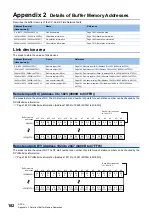
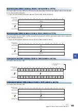
Appendix 2 Details of Buffer Memory Addresses
Appendix 2
Details of Buffer Memory Addresses
Describes the buffer memory of the CC-Link IE Field Network board.
Link device area
The areas to store the values of link devices.
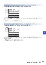
Remote input (RX) (Address 0 to 1023 (0000H to 03FFH))
The areas to store the value of RX. The RX start number and number of points for each station number can be checked by the
RX offset/size information.
Page 184 RX offset/size information (Address 19456 to 19695 (4C00H to 4CEFH))
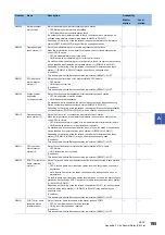
Remote output (RY) (Address 1024 to 2047 (0400H to 07FFH))
The areas to store the value of RY. The RY start number and number of points for each station number can be checked by the
RY offset/size information.
Page 184 RY offset/size information (Address 19712 to 19951 (4D00H to 4DEFH))
Address (Decimal
(Hexadecimal))
Name
Reference
0 to 18975 (0000H to 4A1FH)
Link device area
19456 to 20463 (4C00H to 4FEFH)
Offset/size information
Page 184 Offset/size information
20512 to 20536 (5020H to 5038H)
Own station information
Page 186 Own station information
20544 to 24383 (5040H to 5F3FH)
Other station information
Page 187 Other station information
Address (Decimal
(Hexadecimal))
Name
Reference
0 to 1023 (0000H to 03FFH)
Remote input (RX)
Page 182 Remote input (RX) (Address 0 to 1023 (0000H to 03FFH))
1024 to 2047 (0400H to 07FFH)
Remote output (RY)
Page 182 Remote output (RY) (Address 1024 to 2047 (0400H to 07FFH))
2048 to 10239 (0800H to 27FFH)
Remote register (RWw)
Page 183 Remote register (RWw) (Address 2048 to 10239 (0800H to 27FFH))
10240 to 18431 (2800H to 47FFH)
Remote register (RWr)
Page 183 Remote register (RWr) (Address 10240 to 18431 (2800H to 47FFH))
18432 to 18463 (4800H to 481FH)
Link special relay (SB)
Page 183 Link special relay (SB) (Address 18432 to 18463 (4800H to 481FH))
18464 to 18975 (4820H to 4A1FH)
Link special register (SW)
Page 183 Link special register (SW) (Address 18464 to 18975 (4820H to
4A1FH))
RX
3FFF
RX
3FFE
RX
3FFD
RX
3FFC
RX
3FFB
RX
3FFA
RX
3FF9
RX
3FF8
RX
3FF7
RX
3FF6
RX
3FF5
RX
3FF4
RX
3FF3
RX
3FF2
RX
3FF1
RX
3FF0
RX
F
RX
E
RX
D
RX
C
RX
B
RX
A
RX
9
RX
8
RX
7
RX
6
RX
5
RX
4
RX
3
RX
2
RX
1
RX
0
b0
b1
b2
b3
b4
b5
b6
b7
b8
b9
b10
b11
b12
b13
b14
b15
1023(03FFH)
0(0000H)
Buffer memory
addresses
Each bit corresponds
to 1 bit of RX.
RY
3FFF
RY
3FFE
RY
3FFD
RY
3FFC
RY
3FFB
RY
3FFA
RY
3FF9
RY
3FF8
RY
3FF7
RY
3FF6
RY
3FF5
RY
3FF4
RY
3FF3
RY
3FF2
RY
3FF1
RY
3FF0
RY
F
RY
E
RY
D
RY
C
RY
B
RY
A
RY
9
RY
8
RY
7
RY
6
RY
5
RY
4
RY
3
RY
2
RY
1
RY
0
b0
b1
b2
b3
b4
b5
b6
b7
b8
b9
b10
b11
b12
b13
b14
b15
1024(0400H)
2047(07FFH)
Buffer memory
addresses
Each bit corresponds
to 1 bit of RY.
Summary of Contents for MELSEC Q80BD-J71GF11-T2
Page 2: ......
Page 6: ...4 Disposal Precautions CAUTION When disposing of this product treat it as industrial waste ...
Page 118: ...116 12 MONITORING MEMO ...
Page 140: ...138 14 MELSEC DATA LINK LIBRARY MEMO ...
Page 142: ...140 15 PROGRAMMING 15 1 Precautions on Programming MEMO ...
Page 243: ...241 I U Utility 83 ...
Page 247: ......


