3. SIGNALS AND WIRING
3 - 27
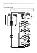
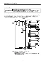
Note 1. Signal can be assigned for these pins with the controller setting.
For contents of signals, refer to the instruction manual of the controller.
2. This diagram shows sink I/O interface. For source I/O interface, refer to section 3.8.3.
3. For the MR-J4 3-axis servo amplifier
4. In the initial setting, CINP (AND in-position) is assigned to the pin. You can change devices of the pin with [Pr. PD08].
5. This signal cannot be used for MR-J4W3-_B.
6. The illustration of the 24 V DC power supply is divided between input signal and output signal for convenience. However, they
can be configured by one.
3.8.2 Detailed description of interfaces
This section provides the details of the I/O signal interfaces (refer to the I/O division in the table) given in
section 3.5. Refer to this section and make connection with the external device.
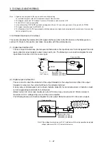
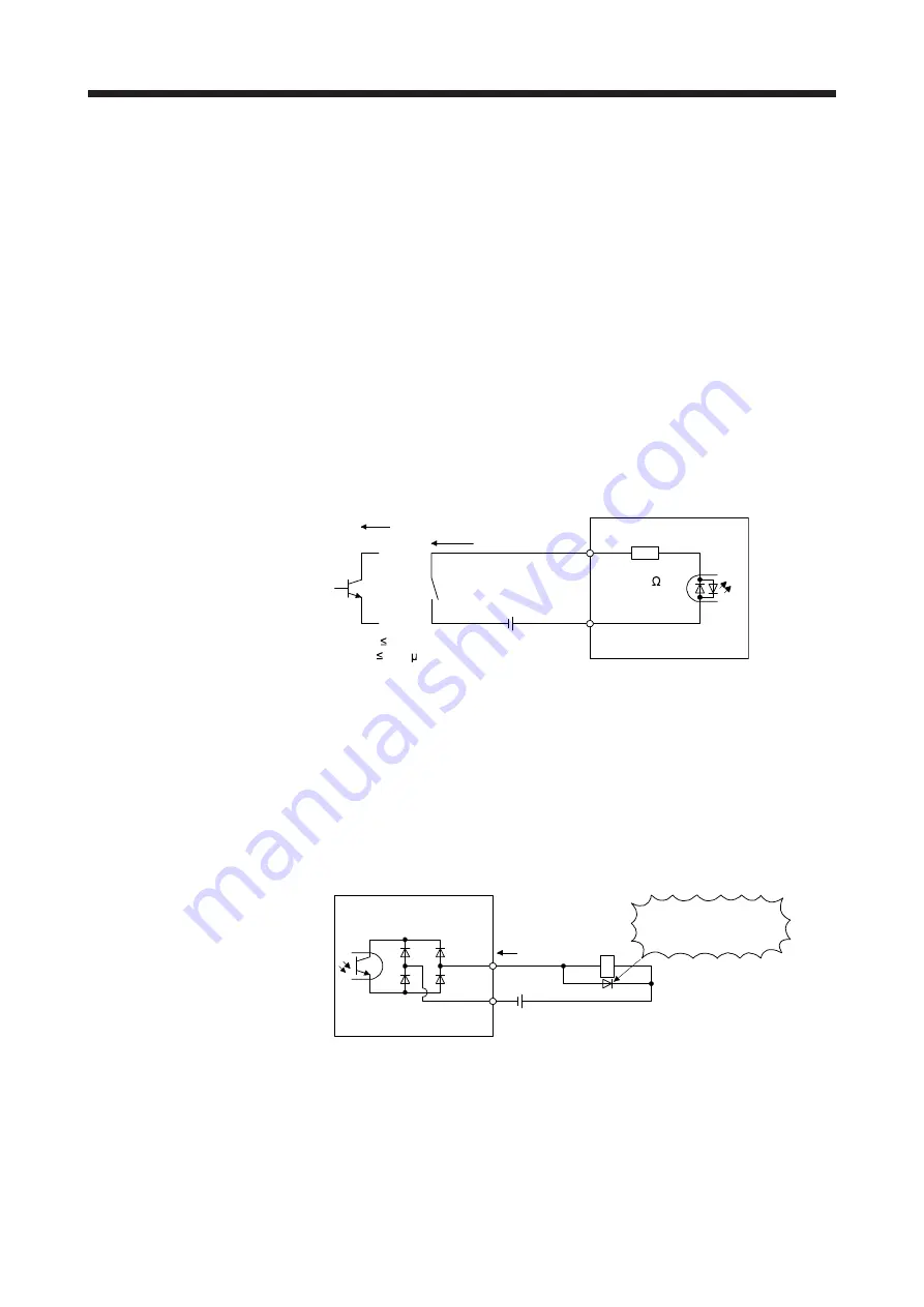
(1) Digital input interface DI-1
This is an input circuit whose photocoupler cathode side is the input terminal. Transmit signals from sink
(open-collector) type transistor output, relay switch, etc. The following is a connection diagram for sink
input. Refer to section 3.8.3 for source input.
Approximately
5 mA
24 V DC ± 10%
MR-J4W2-_B: 350 mA
MR-J4W3-_B: 450 mA
TR
EM2
etc.
Servo amplifier
Switch
For transistor
DICOM
Approximately
5.6 k
V
CES
1.0 V
I
CEO
100 A
(2) Digital output interface DO-1
This is a circuit in which the collector of the output transistor is the output terminal. When the output
transistor is turned on, the current will flow to the collector terminal.
A lamp, relay or photocoupler can be driven. Install a diode (D) for an inductive load, or install an inrush
current suppressing resistor (R) for a lamp load.
(Rated current: 40 mA or less, maximum current: 50 mA or less, inrush current: 100 mA or less) A
maximum of 2.6 V voltage drop occurs in the servo amplifier.
The following shows a connection diagram for sink output. Refer to section 3.8.3 for source output.
If polarity of diode is
reversed, servo amplifier
will malfunction.
Servo amplifier
CALM
etc.
Load
DOCOM
(Note) 24 V DC ± 10%
MR-J4W2-_B: 350 mA
MR-J4W3-_B: 450 mA
Note. If the voltage drop (maximum of 2.6 V) interferes with the relay operation, apply high
voltage (maximum of 26.4 V) from external source.
Summary of Contents for MR-J4W2-0303B6
Page 39: ...2 INSTALLATION 2 8 MEMO ...
Page 97: ...4 STARTUP 4 20 MEMO ...
Page 181: ...6 NORMAL GAIN ADJUSTMENT 6 28 MEMO ...
Page 235: ...9 DIMENSIONS 9 6 MEMO ...
Page 245: ...10 CHARACTERISTICS 10 10 MEMO ...
Page 309: ...13 USING STO FUNCTION 13 14 MEMO ...
Page 365: ...15 USING A DIRECT DRIVE MOTOR 15 24 MEMO ...
Page 389: ...16 FULLY CLOSED LOOP SYSTEM 16 24 MEMO ...
Page 461: ...17 APPLICATION OF FUNCTIONS 17 72 MEMO ...
Page 556: ...APPENDIX App 41 ...
Page 585: ...MEMO ...

