background image

Page 1-7

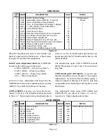
Signal processing circuits are located on the PCB-
SIGNAL. These include:

• Both Tuners
• Video Processing
• Color Processing
• Convergence Circuitry
• Audio Circuitry

The Control Microprocessor is also located on the
PCB-SIGNAL.  To minimize component clutter, this
PCB is double sided.

PCB-APERTURE plugs into the PCB-SIGNAL.

PCB-SVM, Scan Velocity Modulation and PCB-
DBF, Dynamic Beam Formation (or Focus), plug into
the PCB-MAIN.

Note the Flyback Transformer and the HV Capaci-
tance/Resistance Divider are separate components.
The Flyback is mounted on the PCB-MAIN, and CR
Block is mounted on the Main Chassis Frame.

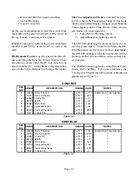
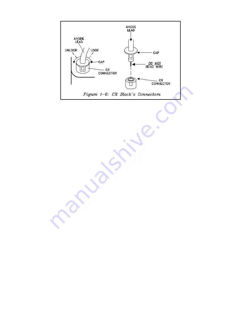
CR Block Connectors
Care must be taken when connecting the HV leads
to the CR Block.  Figure 1-6 illustrates the type of
connector used on the CR Block.  To disconnect a
lead:

1) Rotate the connector cap approximately 90

o

counter clockwise.

2) The cap and the lead can then be pulled from

the CR Block.

To connect a HV lead, reverse the procedure.  When
inserting the lead in the CR Block, insure that the
lead wire is not bent over.
  If the lead is bent inter-
nal arcing occurs and the CR Block can be damaged.

If any audible noise is heard from the CR Block, arc-
ing, sizzling, buzz, etc., check all HV Lead connec-
tions.  This type of arcing can also be seen in the
picture in the form of dotted interference.

Summary of Contents for VS-45605

Page 1: ...cedures Circuit Descriptions Block Diagrams Troubleshooting Techniques Models VS 45605 VS 50605 VS 50705 VS 55705 VS 60705 VS 70705 T 2000 ECHNICAL RAINING MITSUBISHI ELECTRIC MITSUBISHI DIGITAL ELECTRONICS AMERICA INC VZ7 Chassis VZ7 Chassis www mitsubishi tv com ...

Page 2: ... 1 Convergence Mode Description 3 1 CONV MISC Function 3 1 Coarse Adjustment Mode 3 2 Fine Adjustment Mode 3 3 Fine Convergence Adjustment Description 3 4 General Adjustment Procedure 3 8 Section 4 Convergence Circuitry 4 1 Overall Convergence Circuit 4 1 DAC LPF Circuitry 4 3 Amplifier Summing Circuitry 4 4 Convergence Output Amplifiers 4 4 Convergence Control Circuitry 4 7 Section 5 Power Supply...

Page 3: ...cuitry 7 4 VCJ Video Color Internal Path 7 6 Gamma Circuitry 7 8 Blanking Insertion CRT Protect 7 9 RGB Output Amplifiers AKB 7 10 On Screen Display Signal Path 7 12 Section 8 Deflection Circuitry 8 1 Deflection Drive Generator 8 2 Horizontal HV Output Circuitry 8 3 HV Regulation 8 4 Scan Velocity Modulation 8 5 Dynamic Beam Formation 8 6 Vertical Output Circuitry 8 7 Section 9 Audio Circuitry 8 1...

Page 4: ...re labeled DVD Inputs and consist of three video Input jacks plus Right and Left Au dio Jacks The video jacks are denoted as Y Cr and Cb This method allows the baseband Luminance and Color Difference Signals to be coupled directly from a DVD player avoiding any signal degredation that can be caused by chroma modulation and de modulation Basically the signals are Y Luminance R Y and B Y In the NTSC...

Page 5: ...Feature It dis plays complete Crosshatch pattern allowing the user to adjust 64 intersections in the pattern If the con vergence gets too far off the user still has the op tion of selecting Reset to Factory Settings in the initial Convergence menu The AV Memory under Audio Video Settings has five AV Memory selections Standard for typical viewing Daylight for daylight viewing Evening for evening vi...

Page 6: ...1 31 31 27 31 Contrast 63 63 63 45 63 Brightness 31 40 25 31 31 Sharpness 31 31 31 35 35 Color Temp HIGH HIGH HIGH LOW LOW Bass 31 35 35 31 31 Treble 31 35 35 31 31 Balance 31 31 31 31 31 Surround OFF OFF OFF OFF OFF Level Sound OFF OFF OFF OFF OFF Table 1 3 creases both Sharpness and Color adjustments are reduced When Auto Picture is ON the normal adjustment slide is not displayed for Sharpness a...

Page 7: ...layed pressing Info activates the Detail Status Display This display includes Channel Number Channel Name if any SAP STEREO CC and SQV V Chip rating if any Time display Pressing Info in the user s Advanced Convergence Mode displays the functions of the buttons required to set convergence Repeatedly pressing the PIP POP button selects the desired PIP mode The following describes each PIP feature an...

Page 8: ...Down Channel Up and Down becomes Adjust Right and Left AV Reset becomes Cancel Diagnostic Mode The Diagnostic Mode assists the servicer in isolating the source of a problem particularly those problems causing the set to switch OFF shutdown during nor mal operation When the Diagnostic Mode is acti vated the front panel On Off LED flashes a digital code indicating the source of the problem The Diagn...

Page 9: ...n normal operation resumes The two digit codes indicate what malfunction has occurred or that no malfunction has occurred Table 1 4 lists the two digit codes and their meanings Main Chassis PCB Location Figure 1 5 shows the location of the PCBs and ma jor components on the main chassis assembly Two major PCBs comprise the main chassis PCB MAIN PCB SIGNAL Circuitry on the PCB MAIN includes 1 Power ...

Page 10: ...PCB MAIN and CR Block is mounted on the Main Chassis Frame CR Block Connectors Care must be taken when connecting the HV leads to the CR Block Figure 1 6 illustrates the type of connector used on the CR Block To disconnect a lead 1 Rotate the connector cap approximately 90o counter clockwise 2 The cap and the lead can then be pulled from the CR Block To connect a HV lead reverse the procedure When...

Page 11: ...Page 1 8 ...

Page 12: ...low the steps below for the Initial set up 1 Select the MENU display by pressing the MENU button once 2 Press the number buttons 1 2 7 0 in sequence to select the OPTION MENU display 3 Press the ADJUST button to select INITIAL 4 Press ENTER NOTE At this time channel 3 is automatically selected CAUTION On these models E2 RESET activation has been changed To activate the QV button must be pressed wh...

Page 13: ...F TV Listen to STEREO 20 SQV All CH CLEAR deleted TV Bass 50 21 A V NETWORK OFF TV Treble 50 22 LANGUAGE English TV Balance 50 23 NAME THE CHANNELS ALL LABELS CLEARED TV Surround OFF 24 Locked to Input No TV Level sound OFF 25 External Audio System No 11 VIDEO FUNCTIONS 26 Vol change by AV Rec N A TV Tint 50 27 Clock Time TV Color temp High 28 Set Day Sunday After Initalization customer controls a...

Page 14: ...en select the adjustment item Refer to the following pages for the listing of adjustment functions and adjustment items 1 Press the AUDIO button on a remote hand unit to select an adjustment function Each time the button is pressed the Function changes in the following sequence 2 Press the VIDEO button to select a specific Adjustment Item The Item number increases each time the VIDEO button is pre...

Page 15: ...Use Only It enables access to the Service Adjustment Modes by using the VCR buttons on the remote control 1 Activate the Factory Option Menu MENU 1 2 7 0 2 Change the option for DIRECT KEY MODE from OFF to ON 3 Exit the Option Menu Press MENU twice 4 Service Adjustment Modes can now be activated using the following VCR buttons on the remote REWIND activates the Circuit Adjustment Mode PLAY activat...

Page 16: ...in the Convergence adjustment mode These proce dures are described in the Service Manual Section 3 Convergence Adjustments Convergence Mode Description To activate the Convergence Mode press MENU 1 2 5 9 in sequence The screen changes to an in ternally generated Cross Hatch pattern The Cross Hatch is super imposed on the current selected sig nal source To display the Cross Hatch with a black backg...

Page 17: ...only Red is adjustable in the Red Mode and only Blue in the Blue Mode The Adjustment Items under CONV RED and CONV BLUE are shown in Tables 3 3 and 3 4 respectively These adjustments include CONV MISC ADJ NO ABBR DESCRIPTION DATA NOTES 0 HVOL HV DC Control Voltage 140 HV Regulation 1 VINT Interpolation Value 0 NTSC 1 line db 0 Preset 2 HINT Horiz Interpolation Value 0 Req d 0 3 COUT Conv IC Output...

Page 18: ...non blinking cursor The ENTER button toggles the mode between Cur sor Move and Adjust In the Move Mode the AD JUST buttons move the Cursor In the Adjust Mode the ADJUST buttons set the horizontal and vertical position of Red Green or Blue at the current Cur sor position The AUDIO button toggles the Adjust Mode Color Green Red and Blue For a quick reference the Convergence Mode General Procedure is...

Page 19: ...rtical coordinates are assigned to the Cross Hatch pattern The coordinate designations are shown in Figure 3 3 Note that not all the Cross Hatch lines have coordinate designations Fine Adjustments can be performed at the intersections of those lines with coordinates assigned The Vertical coordinates range from 0 to 9 and the Horizontal coordinates from 0 to 8 Vertical coordi nates 0 and 9 and hori...

Page 20: ...usting hori zontal position effects the vertical crosshatch lines at the extreme bottom of the picture The shaded circles in Figure 3 3 indicate the cross hatch intersections that can be adjusted There are a total of sixty four cursor positions to make fine ad justments on the crosshatch NOTES ___________________________________________________________________________ _____________________________...

Page 21: ...e next active intersection on the right ADJUST LFT moves to the next active intersection on the left Adjusting Data Pressing ENTER toggles the Cursor from the Move to the Adjust Mode the Cursor stops flashing The intersection at the Cursor can be adjusted vertically using the ADJUST UP DN buttons or horizon tally using the ADJUST LFT RGT buttons The effect of Green Adjustments is illustrated in Fi...

Page 22: ...t of the V denote the vertical data value for the current Cursor Position The X digits to the right of the H denote the horizontal data value for the Cursor position Both vertical and horizontal data may be either positive or negative ranging from 511 to 511 The digit to the right of the V in dicates the Cursor s current ver tical coordinate position and digit to the left of the H indicates the NO...

Page 23: ... to 1 Incorrect preset data value in the CONV MISC mode Incorrect data values can distort the generated correction signals 2 Incorrect Raster Correction adjustments 3 Coarse Convergence Adjustments are not set to optimum If not set to optimum correction may be out of the Fine Adjust ment mode range NOTES ___________________________________________________________________________ __________________...

Page 24: ...he Service Adjustment Mode VCJ Function Items 24 and 28 Perform Coarse Raster Correction Adjust ments CONV GREEN mode Perform Fine Raster Correction Adjust ments FINE CONV GREEN mode 3 Static Convergence if too far off correction may be out of the range of the Convergence cir cuitry 4 Coarse Dynamic Convergence Adjustment CONV RED mode converge red on the green at the center of the top bottom and ...

Page 25: ...Page 3 10 ...

Page 26: ... Sub Coils in the Deflection Yokes The signals are then amplified and applied to their respec tive Yoke Sub Coils Overall Convergence Circuitry Figure 4 2 shows a simplified diagram of the Over all Convergence Circuitry IC800 is the Convergence Correction Waveform Generator Horizontal pulses are derived from the Horizontal Output stage cir cuitry and vertical pulses from the V Pump terminal on the...

Page 27: ...Page 4 2 ...

Page 28: ...uitry to isolate a problem area Not much can be told from the serial digital signals ex cept that the signals are present DAC LPF Circuitry Figure 4 3 illustrates the circuitry of one Digital Ana log Converter IC and its associated LPF circuitry All three DAC and LPF circuits are the same except for component nomenclature The component no menclature that is given in Figure 4 3 is common to all thr...

Page 29: ...ion Output Amplifiers All three of the amplifi ers are in IC8C01 The amplified outputs are di rected to their respective horizontal sub yoke coil winding For stabilization feedback from the return end of each sub coil is direct to the inverting input of its amplifier The plus and minus 24 Volts supplies furnish power for IC8C01 24 Volts is applied to pins 5 and 10 and 24 Volts to pins 4 8 12 and 1...

Page 30: ...provides a sample of the HV The sample is combined with horizontal sync pulses in the Dynamic Regulator circuit The output of the Dynamic Regulator is routed through resis tive networks to the input of Horizontal Correc tion Output Amplifier The Dynamic Regulator is only used for the Hori zontal Correction Output Amplifiers It is not con nected to Vertical Correction Output Amplifiers ...

Page 31: ...Page 4 6 ...

Page 32: ... 28 and WCLK at pin 27 The two are timing signals for the three Digital to Analog Converter ICs The BCLK signal is applied to pin 16 of each D A Con verter and the WCLK signal to pin 13 The WCLK signal is also used as the Clock signal for the two D type FFs in IC803 the Sync Buffer The WCLK signal is applied the CLK1 and CLK2 inputs of IC803 The PWM1 output at pin 16 of IC800 is the HV Adjustment ...

Page 33: ...Page 4 8 ...

Page 34: ... The Switch Mode Regulator directly generates three Standby Supplies and through the On Off Relay two Switched Supplies STBY 32 Volts STBY 12 Volts STBY 4 Volts SW 18 Volts SW 130 Volts The STBY 12V supply is the source for two addi tional Standby supplies STBY 9 Volts STBY 5 Volts The STBY 12 V supply is also the source for three Switched Supplies SW 12 Volts SW 9 Volts SW 5 Volts The STBY 4 Volt...

Page 35: ...llator running Self Generated DC Supply To maintain oscillation rectification of the signal from the secondary winding at pin 3 of T951 adds to the voltage at pin 4 of the IC Pin 4 is also the Over Voltage Protect input If the voltage exceeds 22 volts the internal circuitry shuts down the oscillator Regulation Feedback Stabilization and rough regulation are provided by feedback from pin 3 of T951 ...

Page 36: ...re not shown in Figure 2 When Q978 is OFF it holds Q976 OFF through the con duction of Q977 With Q976 OFF the SW 12V sup ply is not generated When Q973 is OFF it allows Q972 to conduct A sample of the STBY 12V supply is applied to the base and compared to zener diode D976 in the emit ter circuit The collector voltage is the regulation correction voltage applied to PC951 If the STBY 12V supply is h...

Page 37: ...ge Focus and Screen Voltage the Flyback transformer generates a 230 Volt and a 34 Volt supply The 230 Volt supply is for the RGB amplifiers located on the CRT circuit boards The 34 volt supply sources the Vertical Output cir cuit The Horizontal Output Transformer is the source for the plus and minus 24 Volt supplies used for the Convergence Circuit An additional secondary wind ing is the source fo...

Page 38: ...e of a problem is due to a missing or in correct supply voltage considerable time may be spent tracing the circuitry back to the supply s source The Power Distribution Diagram in Figure 5 4 re duces the time needed to trace a supply s source ...

Page 39: ...age drops below 11 5 volts the oscillator shuts Off 5 If the voltage at pin 4 increases above 22 VDC the internal Over Voltage Protect circuit shut the oscillator Off 6 If the voltage at pin 1 reaches 1 35 VDC the Over Current Protect circuit disables the oscillator 7 A clicking sound indicates the IC is probably defective 8 A chirping sound usually is caused by an excessive load on the Power Supp...

Page 40: ...it is shown above A 100 pin surface mount µPC is the heart of the Control circuitry Primary inputs come from either the front keyboard or the remote Most output commands are communicated by way of four I2 C Buses Besides receiving and generating commands the in ternal circuitry in the µPC Processes Closed Caption signals Generates signals for On Screen Displays Performs V Chip Program Blocking Sec...

Page 41: ...mands The user input command circuitry is shown in Figure 6 2 The front panel buttons are connected in a two column resistive ladder array Each column connects to a Key input on the µPC When a front panel button is pressed the change in voltage at the Key input informs the µPC what command has been entered Remote Control commands are re ceived by the Remote Preamp ampli fied and applied to the RMC...

Page 42: ...controls the remainder of the circuitry in the TV All but two of the controlled circuits shown in Figure 3 are con ventional and need no explanation IC2Y02 DAC IC7V01 Line 21 Decoder IC2Y02 is a Digital to Analog Converter that gener ates voltages controlling PIP Sub Picture Color POP Main Picture Color and voltages controlling the White Balance Gamma circuitry IC7V01 is a Line 21 Decoder Program ...

Page 43: ...ertion inputs at pins 13 14 15 and 16 of the VCJ The sound for the blocked channel is muted in the AV Switch IC2KO1 To monitor the sub picture source the sub picture signal is buffered by Q6C31 and directed over two paths To the NTSC Decoder in IC6C02 To the Video Input of IC7V01 The NTSC Decoder demodulates the video signal and directs the signal to the PIP circuitry It also outputs sub picture h...

Page 44: ...s ON or OFF The 12V supply is directed to the emit ter of Q7A20 through R7A11 and zener diode D7A20 Since Q7A20 is an NPN transistor and the base is tied to ground the transistor conducts The conduction applies negative voltage to pin 20 of the uPC At the same time positive voltage from the 5V Standby supply through R7A08 is directed to pin 20 The combination of the two voltages holds pin 20 LOW T...

Page 45: ... logic at pin 47 of the uPC is controlled by two protect cir cuits monitoring for excess HV and Beam Current To monitor HV a sample of the HV is derived from the resistive divider in the CR Block and is directed to pin 5 of IC501 The sample is amplified in IC501 and di rected to the inverting input of an OP Amplifier at pin 6 of IC502 A stable reference voltage from IC503 is applied to the non inv...

Page 46: ...ry sudden de crease in the voltage at pin 8 of the Flyback The sudden drop in voltage turns Q523 ON The con duction of Q523 turns Q524 ON which holds the base of Q523 LOW When Q523 conducts it turns the set OFF by pulling the P ON command to the power supply LOW Since the circuit latches ON when activated the set cannot be switched back ON AC Power must be removed allowing C593 to discharge before...

Page 47: ...Chip Etc Table 6 1 µPC Specific Function Inputs PIN 3 ABBREV DESCRIPTION 3 AB2 Color Temperature Select 4 AB3 Color Temperature Select 21 OSD BLNK OSD Timing Signal 22 HALFTONE Produces transparent gray background 32 R R OSD signal 33 G G OSD signal 34 B B OSD signal 44 SUB CONT High during Sub Contrast Adjustment 45 BLANK2 Blanks the picture 49 YUV SW Selects the YUV Signal Source 50 POWER Turns ...

Page 48: ...detailed descrip tion is necessary Therefore this section is comprised of only simpli fied diagrams of the various sections of the deflec tion circuity Each diagram is accompanied by a list of key points for that circuit The simplified dia grams are listed below Figure 8 1 Deflect Drive Generator Figure 8 2 Horizontal Deflection HV Output Circuitry Figure 8 3 HV Regulation Figure 8 4 Scan Velocity...

Page 49: ...th the Vertical and Horizontal Drive signal are derived by dividing the output of the 32 x FH 503 4 kHz VCO If the Horizontal Pulse fed back from the FBT to pin 43 of the VCJ is missing the CRTs are auto matically blanked by the VCJ The BGP pulse from pin 55 of the VCJ is directed to the Y Improvement circuitry ...

Page 50: ... derived from the CR Block for the HV Regulation and X Protect circuits The capacitive divider in the CR Block provides the drive signal for the PCB D REG The voltage from pin 8 of the FBT is used by the ACL and Beam Current Protect circuits T519 is the source for the Convergence 24 volt supplies The pulse from Q5AD0 is the Horizontal Yokes drive and is used by the Horizontal Blanking and CRT Prot...

Page 51: ... 9 of IC501 The HV Adjustment voltage from the Convergence circuity is amplified and applied to the non inverting input of the OP Amplifier at pin 10 of IC501 The output of the OP Amplifier controls the conduction of Q501 determining the primary current of T501 The primary current controls the amplitude of the drive signal applied to the FBT ...

Page 52: ...he signal either aids the horizontal deflection signal increasing horizontal scanning velocity or bucks the deflection signal decreasing scanning velocity The SVM effects scanning velocity at sudden video transition from black to white or white to black The scanning velocity is increased in the black area at a transition and decreased in the white area at a transition ...

Page 53: ...oves edge focus A parabolic waveform from the Convergence Waveform Generator is amplified and added to the focus voltage in the Focus VR Block The DC Supply for the DBF Output stage Q5K00 is derived by rectifying the large pulses from the Horizontal Output transistor ...

Page 54: ... three Deflection Yokes The charge on C451 provides additional DC for the Vertical Output stage during vertical retrace The pulse from pin 7 of IC451 is also used for Vertical Blanking and by the Convergence circuitry The feedback network from the Vertical Yokes ground return provides Vertical Linearity and S distortion correction ...

Page 55: ...Page 8 8 ...

Page 56: ...may be moved using the Adjust direction buttons The PIP Size button allows the user to select any of five sizes for the single insert picture In all of the PIP POP modes pressing the PIP POP button after 10 seconds terminates the PIP mode Familiarity with the Video Color signal path in the various PIP POP modes helps isolate problems to a specific section of the circuitry The following lists key p...

Page 57: ...Page 7 2 ...

Page 58: ...als are directed to the PIP POP cir cuitry in IC6P01 The sub picture video signal from IC2K01 is applied to an NTSC Decoder in IC6C02 The sub picture YUV output signals are also applied to IC6P01 In IC6P01 the main and sub picture signals are pro cessed and combined to form the Y U and V signals for the Side by Side picture The Y signal is directed through IC60Y1 and Aperture circuit to the Main Y...

Page 59: ...are per formed to match color of the Side by Side main pic ture to that of the sub picture IC6C02 is the Sub Picture NTSC Decoder Since the sub picture signal is composite video the inter nal input signal path in the IC differs from that of the main picture Decoder The sub picture Video is in put to the IC at pin 13 and then takes two paths 1 Through a Chroma Trap removing chroma signal and then t...

Page 60: ...V signals to digital and writes them into memory The memory is then read in the sequence required to produce the signal for the Side by Side pictures The signals are converted back to analog and directed out the YUV outputs of the IC IC6Y01 directs the POP Y signal to pin 63 of the VCJ The signal selection of IC6Y01 is controlled by the PIP SW line from the Control circuitry A HIGH selects the POP...

Page 61: ... Blank signal input at pin 5 of the VCJ controls the insertion of the sub YUV signals into the main YUV signal In the POP mode VZ7 only the combined main and sub picture Y signals are input to the VCJ at pin 63 The POP UV signals are input to pins 10 and 8 of the VCJ The logic at pin 5 goes HIGH from the PIP SW line selecting pins 63 8 and 10 as the ac tive inputs to the VCJ When DVD Component is ...

Page 62: ...round for certain on screen dis plays The amplitude of the RGB video signals is re duced by 1 2 in the background area of the OSD This dims the video in the background The YS Switch inserts On Screen Display OSD information into the Main Signals OSD signals are applied to pins 14 15 and 16 The YS signal at pin 13 times the insertion of the OSD The signal path for the OSD sources is provided at the...

Page 63: ... and green This results in yellowish cast in bright white areas of the picture The circuitry in IC2H00 increases the amplitude of the blue signal at high brightness levels so its light output matches the red and green The DC voltages at pin 1 2 3 4 6 and 7 determine at what point and how much blue signal amplitude is increased The DC voltages are derived from resistive dividers and are fixed at pi...

Page 64: ...d to the base of Q522 and a Vertical Sawtooth from the Vertical Yokes ground return circuit is applied to base of Q401 The conduction of the two tran sistors holds their collector voltages below the zener point of D456 If either transistor stops con ducting its collector voltage exceeds the zener point and Q2W62 is driven into con duction blanking all three CRTs Spot Killer circuitry momentarily t...

Page 65: ...al to the Green CRT cathode The rest of the circuitry shown on the PCB CRT G is part of the AKB Circuit AKB Circuitry The AKB circuitry automatically adjusts the CRTs Cutoff Bias point if CRT characteristics change with age To detect a change in CRT characteristics the circuitry automatically checks the point at which each CRT starts to conduct and compares it to the previ ous Cutoff setting To de...

Page 66: ...include A bright white raster that can exceed beam current limits causing the set to shut down No raster Delayed raster when first turned on Note Similar symptoms can be caused by improp erly adjusted Screen Controls Accurately setting the CRT Cutoff Adjustments is critical for proper operation and performance Refer to the Service Manual to perform the procedure Disabling the AKB loop helps simpli...

Page 67: ... accessed Convergence Adjustment Mode IC700 Control Microprocessor Generates all other OSD graphics including all Menus Closed Captioning and other informational displays The Red Green and Blue signals output from the two sources are combined within the OR gates in ternal to IC703 to form the RGB signals applied to the VCJ Blanking signals used to time OSD insertion are combined separately before ...

Page 68: ...modulation and Stereo SAP decoding User sound adjustments such as Volume Treble and Bass are performed in the this IC controlled by the Main SDA line from the uPC Control Circuitry The outputs at pin 6 and pin 47 of IC3A01 are di rected over two paths 1 To the Power Amplifiers in IC301 and then to the Speakers and 2 back to IC2K01 at pins 29 and 31 The sound signals applied to the Audio Output Jac...

Page 69: ...Page 9 2 ...

Reviews: