Page 5-3
Over Current Protection
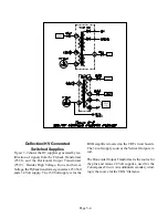
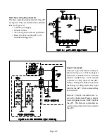
Pin 1 of IC951 is also the Over Current Protect in-
put. The internal FETs ground return is at pin 2 of
the IC. The voltage drop across R955 and R956
indicates the FETs current, and is coupled through
R953 to pin 1 of the IC. The Over Current Protect
circuit is activated if the voltage at pin 1 of the IC
exceeds 1.35 volts.
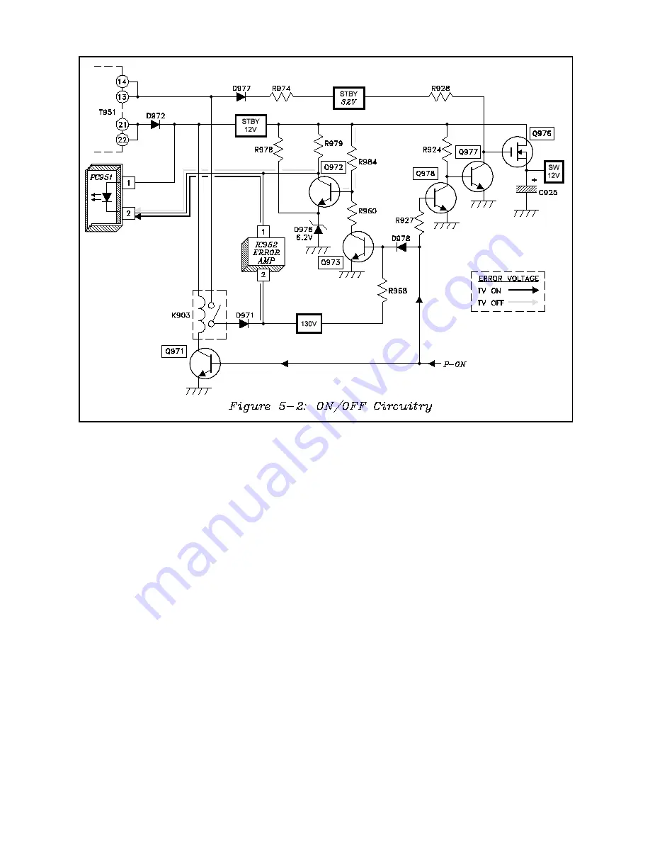
ON/OFF Circuitry
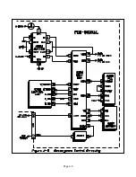
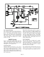
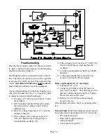
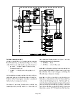
Figure 5-2
shows the ON/OFF circuitry in the VZ7
chassis. The P-ON line from the Control µPC is the
ON command. When the set is OFF, the line is LOW,
holding Q971, Q973 and Q978 OFF.
Set OFF Operation
With Q971 OFF, the Off/On Relay is open and the
130V and 18V supplies are not generated. The 18V
Relay contacts are not shown in
Figure 2
. When
Q978 is OFF, it holds Q976 OFF through the con-
duction of Q977. With Q976 OFF, the SW 12V sup-
ply is not generated.
When Q973 is OFF, it allows Q972 to conduct. A
sample of the STBY 12V supply is applied to the
base and compared to zener diode D976 in the emit-
ter circuit. The collector voltage is the regulation
correction voltage applied to PC951. If the STBY
12V supply is high, Q972 conducts more decreasing
the correction voltage. If the supply is low, the cor-
rection voltage increases.
Set ON Operation
When the P-ON line goes HIGH, Q971 conducts
closing the ON/OFF Relay. Q978 and Q973 are
driven into conduction. The conduction of Q978
turns Q977 OFF, which allows Q976 to conduct,
generating the SW 12V Supply.
The conduction of Q973 turns Q972 OFF. The regu-
lation correction voltage is now derived from the
130V supply through the Error Amplifier in IC952.
Summary of Contents for VS-45605
Page 11: ...Page 1 8 ...
Page 25: ...Page 3 10 ...
Page 27: ...Page 4 2 ...
Page 31: ...Page 4 6 ...
Page 33: ...Page 4 8 ...
Page 55: ...Page 8 8 ...
Page 57: ...Page 7 2 ...
Page 69: ...Page 9 2 ...


