background image

Technical Training and
Troubleshooting Guide

T
 2002

  ECHNICAL
RAINING

www.mitsubishi-tv.com
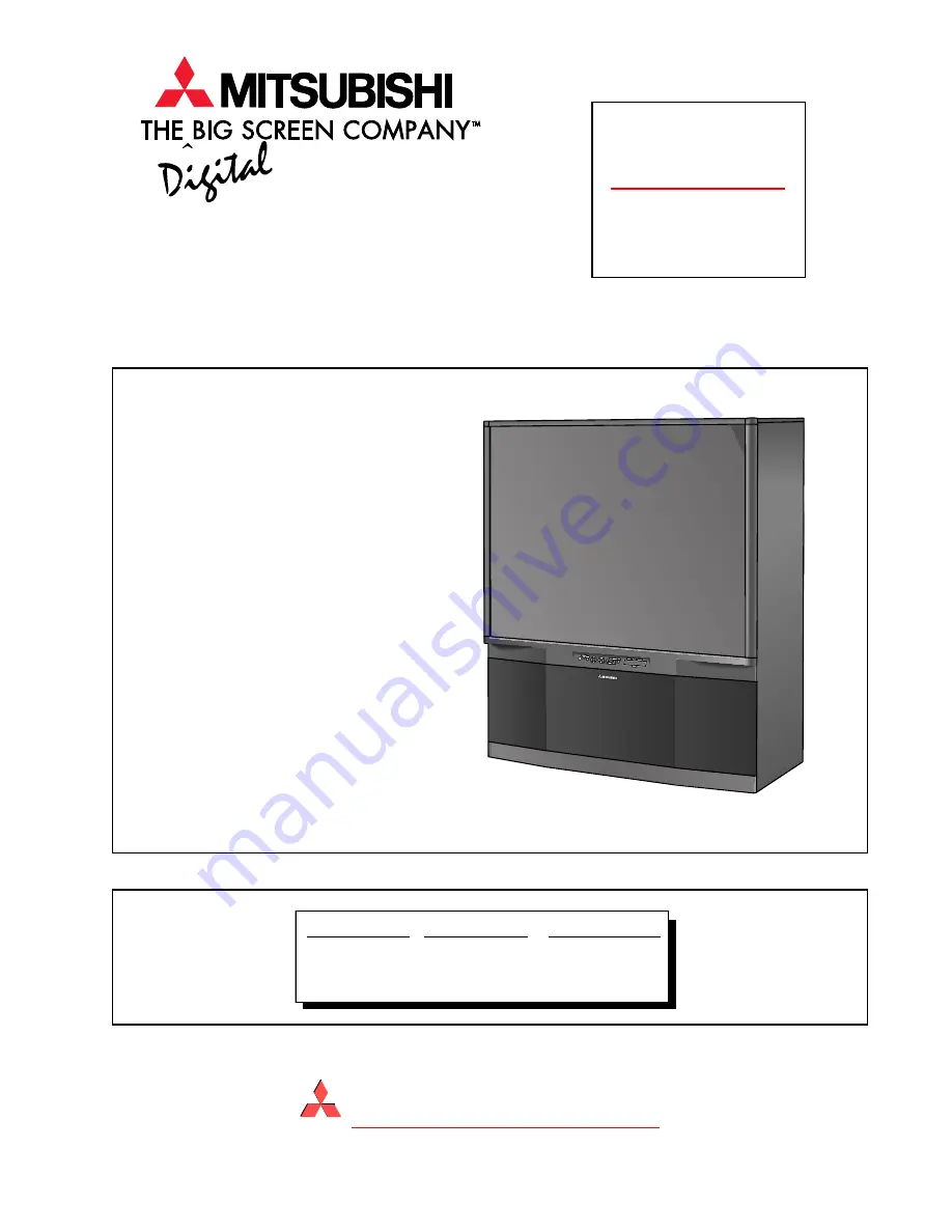
V20

Chassis

V20

Chassis

V20A Chassis

V20C Chassis

V20C+ Chassis

VS-50111

WS-48311

WS-55411

VS-60111

WS-55311

WS-65411

WS-65311

WS-73411

Digital Ready
Projection Television

MITSUBISHI ELECTRIC

MITSUBISHI DIGITAL ELECTRONICS AMERICA, INC.

Summary of Contents for VS-50111

Page 1: ...RAINING www mitsubishi tv com V20 Chassis V20 Chassis V20A Chassis V20C Chassis V20C Chassis VS 50111 WS 48311 WS 55411 VS 60111 WS 55311 WS 65411 WS 65311 WS 73411 Digital Ready Projection Television MITSUBISHI ELECTRIC MITSUBISHI DIGITAL ELECTRONICS AMERICA INC ...

Page 2: ...x ...

Page 3: ...ooting Guide Table of Contents Introduction i Chapter 1 Chassis Layout Servicing 1 1 Chapter 2 Adjustments 2 1 Chapter 3 Power Supply 3 1 Chapter 4 Control Circuitry 4 1 Chapter 5 Video Color Circuitry 5 1 Chapter 6 Deflection and High Voltage Circuitry 6 1 Chapter 7 Convergence Circuitry 7 1 Chapter 5 Sound Circuitry 8 1 ...

Page 4: ...x ...

Page 5: ...8chassis Tosimplfythechassis thenumberof stand upPCBshasbeenreduced So manyofthesame circuitshavebeenconsolidatedontolargerPCBs This manualwillexplainthemajorfeatureandcircuitrydif ferences For the areas that are relatively the same refer to the V17 or V18 Training Manual The Service Menu Codes have been changed for the 2002 Model Year Table 1 lists the Menu Codes for all recentMitsubishiChassis V...

Page 6: ...V20 Chassis Technical Training and Troubleshooting Guide ii ...

Page 7: ...Double Convergence Amps Decoders Generator 480i to 480p DBF Table 1 PCB Functions NOTE The locations of PCB MAIN and PCB POWER have been reversed compared to previous chassis As mentioned in the Introduction the main differ ence between the V20 chassis and the V17 and V18 chassis is the reduction of stand up PCBs This means many circuits have been moved from individual PCBs onto larger PCBs Table ...

Page 8: ...essibility The RF Connectors have been strengthened in the V20 by adding a support plate When replacing the PCB Signal or RF Switch assembly be sure the plate is installed on the connectors as shown in Figure 3 The High Voltage Anode Lead Connector has been enhanced in the V20 Spring tension between the lead and the FBT has been added to help secure the connection This changes the removal procedur...

Page 9: ...ont panel INPUT and MENU buttons at the same time and holding for 5 seconds activates the Error Code Mode The LED flashes denoting a two digit Error Code or indicating no problem has occured since the last Power Off Error Code Description 12 No error has occurred 21 X Ray Protect circuit 22 Short Protect circuit 23 Horizontal Deflection failure 24 Vertical Deflection failure Note The front panel b...

Page 10: ...V20 Chassis Technical Training and Troubleshooting Guide 1 4 ...

Page 11: ...hegeneralalignmentproceduresfortheV20chassisremain the same as previous HD ready chassis For your convenience the following procedures are provided in this chapter Forspecificalignments refertotheServiceManual Initial Settings Option Menu Circuit Adjustment Mode Convergence Adjustment Mode Adjust Items List Initial Data Settings ...

Page 12: ... 5 Daylight Savings Time Applies Unlock Time N A TV Balance 0 5 Clock Time N A TV Surround Off Set Day N A Video Mute On TV Listen To Stereo Black Enhancement On TV Level Sound Off Closed Captions On if Mute VIDEO SETTINGS CC Background Gray TV Contrast 1 Timer Off TV Brightness 0 5 Antenna ANT A Set Time 12 00PM TV Sharpness 0 5 Channel 3 Set Day Everyday TV Color 0 5 Memory Deleted Device Ant A ...

Page 13: ... Brightness Mid Mid Mid Mid Sharpness Mid Mid Mid Mid Color Mid Mid Mid Mid Tint Mid Mid Mid Mid Color Temp High High High High Video Noise Stnd Stnd Stnd Stnd Image type Video Video Video Video TV VSM Sharpness On On On On Bass Mid Mid Mid Mid Treble Mid Mid Mid Mid Balance Mid Mid Mid Mid Surround Off Off Off Off Listen To Stereo N A N A N A Level Sound Off Off Off Off AV Memory Initial Settings...

Page 14: ... the following pages for the listing of adjustment functions and adjustment items 1 Press the AUDIO button on a remote hand unit to select an adjustment function Each time the button is pressed the Function changes in the following sequence 2 Press the VIDEO button to select a specific Adjustment Item The Item number increases each time the VIDEO button is pressed C Changing Data After selecting a...

Page 15: ...NTSC the SD mode is activated If the signal source is HD 1080i the HD mode is activated 3 Activating the HD mode when no HD signal is available Activate the Factory Option Menu MENU 2 2 7 0 Use the Adjust keys to select DTV Port and press Enter to change the setting to 1080i Sequence Auto 480i 480 p 1080i Ignore any loss of sync while changing modes Exit the Option Menu Press MENU twice Select the...

Page 16: ...se AUDIO button to select a Sub Function 2 Use the VIDEO button to select an Adjustment Item 3 Use the ADJUST buttons to change data F FINE CONV Press 4 Sub Functions This mode is used to perform Fine Raster Correction and Fine Red and Blue Convergence Adjustments There are three Sub Adjustment Functions selected with the AUDIO button FINE GREEN a Green Crosshatch is displayed for Fine Raster Corr...

Page 17: ...e 480i 480p 1080i Adjustment 1 SCT Picture Gain control 0 63 42 42 42 Sub Contrast 2 SBRT Sub Brightness 0 63 20 20 20 Black Level 3 SCON Sub Contrast 0 15 7 7 7 Preset 4 RDRH R Drive H temp 0 63 31 31 31 White Balance 5 GDRH G Drive H temp 0 63 41 41 41 Preset 6 BDRH B Drive H temp 0 63 31 31 31 White Balance 7 CTRH R Cutoff H temp 0 63 31 31 31 8 CTGH G Cutoff H temp 0 63 31 31 31 Preset 9 CTBH ...

Page 18: ...trol 0 63 19 3 YDRM Main Y Gain 0 63 12 SUB MATRIX MENU 2 2 5 7 Item Abbrev Description Range Initial 1 TNTS Main Tint Control 0 63 28 2 COLS Main Color Control 0 63 30 3 YDRS Main Y Gain 0 63 12 4 VPDS U signal DC Control 0 15 7 5 UPDS V signal DC Control 0 15 7 Data Data CONV MISC MENU 2 2 5 9 6 Item Abbrev Description Range SD HD 1 HVOL HV Adjust 0 352 150 150 2 VCNT V saw amplitude 0 127 29 29...

Page 19: ...arity 195 170 140 125 150 170 180 170 140 125 150 150 150 150 220 190 6 HWID Width 22 30 5 0 0 0 0 0 5 0 0 0 0 0 0 0 7 VKEY Vert Keystone 100 85 15 87 70 90 100 95 15 87 90 70 90 70 100 110 8 VWID Height 0 16 0 0 0 0 0 0 0 0 0 0 0 0 0 0 9 VLIN Vert Linearity 0 0 0 0 20 20 0 0 0 0 0 0 0 0 0 0 10 TBPC Top Bottom PC 200 169 150 150 20 20 20 20 150 150 20 20 20 20 20 20 11 SDBW Side Bow 0 0 0 0 30 30 ...

Page 20: ...V20 Chassis Technical Training and Troubleshooting Guide 2 10 ...

Page 21: ...but there are differences The largestdifferenceisintheStandbyRegulatorcircuitry A different Regulator IC is used generic TNY264 Regulation in previous models was by Pulse Width Modulation PWM where the duty cycle of the regu lator output was varied to maintain a constant out put voltage The TNY264 is an Off Line Switcher that regulates by enabling or disabling output from an internalMOSFET Figure1...

Page 22: ...s are generated as long as power is applied to the IC The Clock signal triggers the start of each cycle Duringtheclocksignal theENinputvoltageat pin 4 is checked The voltage at the EN input is con trolled by feedback from the DC output supply If pin 4 is 1 volt or higher the S input of an internal FF is driven High through the Enable AND gate The Q output of the FF goes High turning On the MOSFET ...

Page 23: ...the IC include Low power consumption 9V 170 ma is typical Usinga132kHzoscillatorfrequencyallowsa reducedtransformersize Standby Regulator Circuit Figure3illustratesaSimplifiedVersionoftheStandby Regulator Circuit The full wave rectifier D9A21 and D9A20 supplies DC power to pin 5 of IC9A20 The voltageatpin5suppliespowerforboththeinternalos cillator and the MOSFET C9A28 at pin 1 serves as a bypass f...

Page 24: ...4 of IC9A20 When the voltage at pin4islessthan1voltatthestartofanoscillatorcycle no drive is applied to the internal MOSFET This re sultsinloweringthevalueofthe9VSsupply Figure 4 shows the power distribution of the Standby supplies The 9VS supplies power for the On Offcircuitry ACOFF detection circuit RFSwitch CRTProtect circuit IC9C21 5VS Regulator The 5VS supply powers the Microprocessor circuit...

Page 25: ...eneratingapproximately20volts The20volts is directed to the collector of Q9A50 and the collector of the Photo Transistor at pin 8 of PC9A50 When the set is switched On the P ON line from the ControlCircuitgoesHighturningQ9A51On which Closes relay K9A50 Lights the LED at pins 5 and 6 of PC9A50 K9A50shortsoutthecurrentlimitingresistor R9A02 ThelightfromtheLEDturnsOnthePhotoTransistorat pins 7 and 8 ...

Page 26: ... 12V The 110V is the source for a 30V supply The 24V supplyisthesourceforSwitched12Vand5Vsupplies Two9Vsuppliesarederivedfromthe12Vsupply The 5V supply is the source for two 3 3V supplies The17VsupplyistheDCsourcefortheAudioOutput IC In the V20A chassis audio output wattage is re duced from 10 Watts to 5 Watts Therefore the 17V supply is reduced to 12V To reduce the 17V to 12V a different secondar...

Page 27: ...3 User commands originate from front panel or remote control 4 Status Inputs keep the µPC aware of current operating conditions 5 µPC output commands control the TV s circuitry Basic Operating Requirements TheµPCbasicoperatingrequirementshavenotchanged DCsupply Ground returns for the internal circuitry Clock Signal s for timing Method of resetting the µPC Figure 1 illustrates the basic µPC require...

Page 28: ...n 11 of the µPC The watch dog counter is not reset Thecounterreachesits maximumcount A Reset pulse is generated The µPC resets to clear the lock up Input Commands The Input Command circuitry is also similar to that in previousmodels asshowninFigure2 Thefrontpanel buttonsareconnectedinatwo columnresistiveladder configuration EachcolumnisconnectedtoaKeyScan KSC input on the µPC Pressing a button cha...

Page 29: ... data lines Figure 3 shows the serial data lines used in the V20 chassis Four I2 C data lines are used EE SDA MN SDA C SDA and SUBCCD SDA Of courseeachI2 Cdatalinehasacorrespondingclock SCL line to time data transfer The EE SDA line transfers programming and ser vice data to and from two EEPROMs The added EEPROM on PCB TERMINAL stores adjustment data for the Main and Sub NTSC Decoders This include...

Page 30: ...single direction system consisting of D IN D OUT and SCLK D OUT transmits data from the µPC to the PCB DOUBLER D IN transmits data from the PCB DOUBLER to the µPC SCLK times the data transfer V Chip Control Figure4illustratestheV ChipControlcircuitry Main pictureV ChipprocessingisinternaltotheControlµPC IC7A00 Main picture video is input at pin 100 of IC7A00 and the internal circuitry determines t...

Page 31: ...are listed in Table 1 giving the inputabbreviation description purpose andthesource ofthatspecificsignal Parallel outputs are mainly control logic or signals such as On screen display signals Parallel outputs are given in Table 2 along with the description and the destination for that signal IC7A00 Microprocessor Inputs PIN ABBREV DESCRIPTION SOURCE 6 SD2 Sub Tuner Sync ÍQ1B32 7 SD1 Main Tuner Syn...

Page 32: ... On command Î KE 14 Î KH 6 ÎQ9A51 52 ASIC CS Doubler Chip Select Î EB 19 53 FON Horizontal scan freq Logic ÎIC2V00 23 54 F1 Horizontal scan freq Logic ÎIC2V00 24 56 F31K Adjusts Horiz DC Supply Î KD 3 ÎQ5A35 Q5A07 57 DEFL MUTE Reduces Horiz DC during sweep changes Î KD 4 ÎQ5A08 74 VCHIP RST V Chip Reset ÎIC2VO1 4 78 AUDIO RESET Audio Reset ÎIC3A01 16 79 3D RESET 3DYC Reset Î JB 19 ÎIC2MOO 57 80 MU...

Page 33: ...mproved Line Doublercircuitry Thecircuitrycanprocess480i NTSC orComponent 480pand1080ianalogsignalformats All component YCbCr inputs are capable of receiv ing1080isignals The picture is displayed in either 480p or 1080i scan format Improvements in the PCB DOUBLER Line Doubling and POP PIP circuitry enables any compat ible signal source to be selected as either the main or subpicture ...

Page 34: ...itry select signals from the Decoders or a YCbCr com ponentinput The selected signals are directed to PCB SIGNAL TheamountofVideo ColorcircuitryonPCB SIGNAL hasbeenreduced itconsistsmainlyof MainandSubTuners A PIP Switch IC Video Color Jungle VCJ All Main and Sub picture signals from PCB TERMINAL are directed though PCB SIGNAL to PCB DOUBLER ThecircuitryonPCB DOUBLER basicallyperformsthreefunction...

Page 35: ... in the PIP Switch circuit Ifanotherdisplayformatisselected oraPOPfunction is activated the shape of the main picture has to be changed To do this the main picture signal must be processedbytheDOUBLERcircuitry ThenanyPOP PIPinsertionoccursintheDOUBLERcircuitryandthat signal is selected by the PIP Switch and applied to the VCJ The circuitry in the VCJ converts the YCbCr signals to the RGB format an...

Page 36: ...80p or 1080i format At the inputs to the Decoders these signal are directed 480p 1080i sync circuitry for sync pulse ex traction Main C signal from the 3DYC circuit is applied di rectly to the Main Decoder Each Decoder converts it srespectiveinputsignal s totheYCbCrformat The output of each Decoder is directed to it s respective YCbCr Switch IC There are three addition sets of signal inputs to eac...

Page 37: ...en hances the YCbCr signals improving picture quality The signals are then convertedtoRGBanddirectedtotheir respective CRTs CRT RGB Circuitry Figure 4 shows the CRT s RGB Am plifiercircuitry EachCRT srespective signal is amplified in an IC either IC6R01 IC6G01 or IC6B01 and ap plied to that CRT s cathode The output at pin 7 of the three RGB Amplifier ICs indicate the point at which that CRT starts...

Page 38: ...V20 Chassis Technical Training and Troubleshooting Guide 5 6 ...

Page 39: ... Top Box is RGB sync is either on the G signal or separate horizontal and vertical sync are output from the box SyncSelectcircuitryselectsMainpicturesyncsource The selected output is used to synchronize the Hori zontalandVerticalDeflectionGenerators Ifthesource signal is 480i horizontal sync is doubled before syn chronizingtheHorizontalDriveGenerator HorizontaldeflectiondriveisamplifiedbytheHorizo...

Page 40: ...hesourcesignalis480ifor mat IC2L01extractscompositesync combinedhori zontal and vertical sync from the Y signal when the source is 480p or 1080i IC2N00 selects 480p 1080i sync from IC2L01 or separate 1080i H and V sync from the DTV inputs IC2P01 selects 480p or 1080i sync from IC2N00 or 480i sync from IC2L00 The selected sync is directed to the Doubler circuitry Iftheselectedsourceis480i thenumber...

Page 41: ...rates the Horizontal Deflection Drive and Output circuitry Horizontal drive signal from the VCJ is amplified by Horizontal Drive circuitry comprised of transistors Q2V40 Q5A40 Q5A33 Q5A39 and Q5A32 The output from Q5A32 is directed to Q5A31 the Horizontal Output transistor The output from Q5A31 takes three paths 1 TothehorizontalwindingsintheDeflection Yokes 2 Through C5A34 and Q5A37 to the HV Dri...

Page 42: ...07into conduction reducingthebasevoltageofQ5A06 which reduces the DC supply to the Horizontal Output The H MUTE line from the µPC and Q5A08 reduce the DC supply during scan frequency change by the samemethod The DC supply for the Horizontal Drive transistor Q5A32 is derived from the Horizontal Output DC supply through R5A36 R5A37 and Q5A34 In the 31 5kHzmode theDCsupplyforQ5A32woulddrop since the ...

Page 43: ... resistive divider in the Flyback and is output at pin 13 The HV sample is applied to the non invertinginputofanOP AmpinIC5A01 TheHVADJ voltageinappliedtotheinvertinginputofasecondOP Amp in IC5A01 The outputs of both OP Amps are combined and directed to pin 4 of IC5A00 DO NOT measure the HV DC FB voltage at pin 13 of the T5A51 The meter may load down the internal resistivedivider resultinginexcess...

Page 44: ...sourcesisappliedtoaninputof an OP Amp in IC5A02 The second input of each OP Amp is connected to a specific reference The outputs of all three Op Amps are tied together at the X Rayline The X Ray line is normally High If any of the moni tored sources exceeds its specific reference the X RaylineispulledLow shuttingOfftheTV The connection from the source of Q5A51 to pin 5 of IC5A00providesfurtherprot...

Page 45: ...topin1ofIC4B01 providelinearityandS correction The vertical saw tooth across R4B12 and R4B10 is directed back to pin 35 of IC2V00 Pin 35 is the V Protect Input if the saw tooth is missing IC2V00 removes all RGB drive to the CRTs Deflection Loss Detection To prevent damage to the CRTs the TV must shut Off if deflection is lost The De flection Loss Detection circuit is similar to previous models as ...

Page 46: ...evalueofthemostsignificantdigit MSD of the code first then flashes the value of the leastsignificantdigit LSD ofthecode Theerrorcode is repeated 5 times If the LED flashes twice pauses then flashes 4 times the Error Code is 24 The code specifiesthereasontheTVswitchedOff Table1Lists the possible error codes To activated the Error Code press the front panel In put and Menu buttonsatthesametime andho...

Page 47: ...signals in the Amplifiers hence the name Summing Amplifiers The correction signals are amplified by Output Am plifiers and are directed to the sub coils in their re spective Deflection Yokes Thisisthesamebasiccircuitryusedinthelastfewchas sis types There are only two major differences in V20 Convergence circuitry compared to that in the V19 1 In the V20 the Waveform Generator is on the PCB SIGNAL ...

Page 48: ...rcuitryduringchannelorinputchange and duringOn Off C BUSY Allows IC8D00 to notify the µPC if it is busy C ACK Acknowledgmentline allows notification to the µPC that a command was received C RST Convergence Reset IC8D00alsogeneratesthesignalsfortheinternalcross hatch pattern These are the C OSDR C OSDG and C OSDB signals that are directed to the VCJ The C BLK signal from IC8D00 times the crosshatch...

Page 49: ...F Summing Amps Figure 2 illustrates the LPF and Summing Amplifi ers The circuitry consists of three ICs IC8E00 IC8E01 and IC8E02 Each correction signal from IC8D00 goes through two stages of amplification 1 The first stage is part of the LPF 2 The second stage is the Summing Amplifier Green horizontal and vertical correction signals are added to the Red and Blue Summing Amplifier in puts ...

Page 50: ...stheConvergenceOutputcircuitry This circuitry is basically the same as used in the past The correctionsignalsareamplifiedanddirectedtotheSub Vertical and Sub Horizontal coils in their respective DeflectionYokes TheConvergenceOutputCircuitry isshowninFigure3 Itincludespinnumbersandcom ponentnomenclature ...

Page 51: ...rearedifferences Thedifferencesinclude No sub picture sound output is featured The 4 5 mHz Sound I F output from the Main Tuner is the TV s sound source A Sound Detector external to the Tuner has been added There are no Service Sound Adjustments these areautomatic In the Block Diagram three individual blocks repre sent the Sound I F Detector MCS Decoder and Audio Control circuits All three of the ...

Page 52: ... output at two sets of out put on IC2K00 The main right and left signal output from pins 43 and 45 are directed to Audio Control circuitry on PCB SIGNAL Therightandleftoutputsatpins52and54ofIC2K00 are the Fixed Level outputs and are directed to Moni tor Output Select Circuitry The Monitor Output Se lect Circuitry is comprised of IC3K00 and IC3K01 The two ICs select either the fixed level output fr...

Page 53: ...d to pin 50 of IC3A01 The internal cir cuitry in IC3A01 Detects the Sound I F signal and performs MCS Decoding output TV right and left signals TheTVrightandleftsignalaredirectedtothe AVSwitchcircuitryonPCB TERMINAL The selected signals from the AV Switch circuit are di rected back to IC3A01 at pin 44 and 45 The signals passthroughinternalAudioControlcircuitry allowing user adjustment to be made T...

Page 54: ...revious models IC3E01 amplifiestherightandleftsignals andprovidespush pull drive output signals for the set s speakers Note the DC Supply for IC3E01 is 17 volts for all models except VS 50111 and VS 60111 In these two models the DC supply is reduced to 12 volts All models except VS 50111 and VS 60111 use 10 watt speakers these two models use 5 watt speakers ...

Reviews: