


3-3
V20 Chassis Technical Training
and Troubleshooting Guide
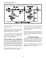
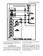
If the load is heavy, the maximum current level is in-
creased, supplying more power to the transformer.
Under light load conditions, the current limit is de-
creased. This allows the FET to be turned On and Off
at a rate that is above the audio frequency range. This
reduces any noise due to the lower On/Off MOSFET
output switching rate.
Other features of the IC include:
• Low power consumption, 9V @ 170 ma is
typical.
• Using a 132 kHz oscillator frequency allows a
reduced transformer size.
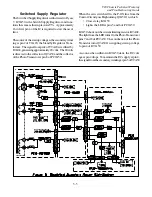
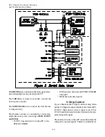
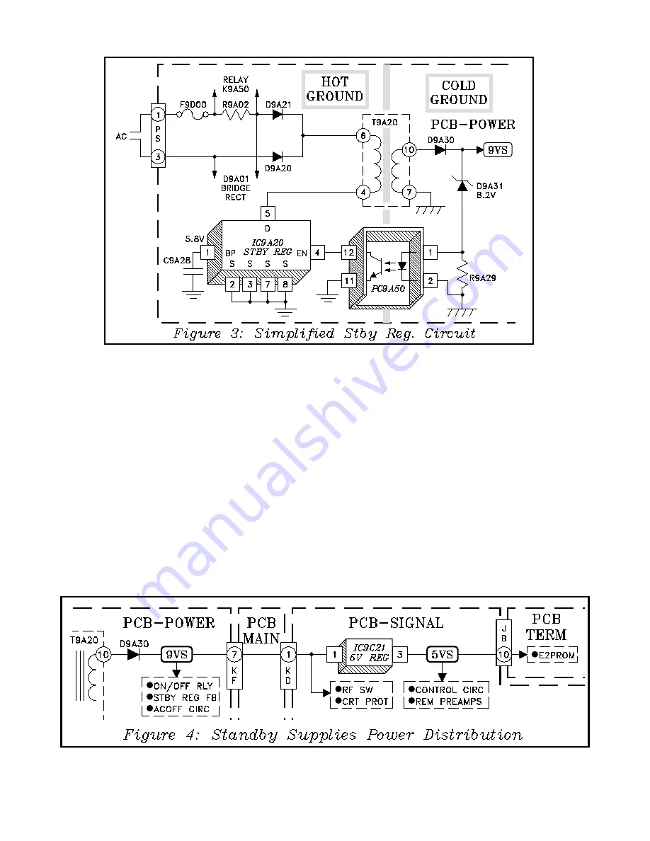
Standby Regulator Circuit
Figure 3
illustrates a Simplified Version of the Standby
Regulator Circuit. The full wave rectifier, D9A21 and
D9A20, supplies DC power to pin 5 of IC9A20. The
voltage at pin 5 supplies power for both the internal os-
cillator and the MOSFET. C9A28 at pin 1 serves as a
bypass for an internally generated 5.8 Volt supply.
D9A30 rectifies AC from a secondary winding of
T9A20, generating a 9VS supply. This is the source for
all standby supplies in the TV. The 9VS supply is also
monitored for regulation.
Summary of Contents for VS-50111
Page 2: ...x ...
Page 4: ...x ...
Page 6: ...V20 Chassis Technical Training and Troubleshooting Guide ii ...
Page 10: ...V20 Chassis Technical Training and Troubleshooting Guide 1 4 ...
Page 20: ...V20 Chassis Technical Training and Troubleshooting Guide 2 10 ...
Page 38: ...V20 Chassis Technical Training and Troubleshooting Guide 5 6 ...