


• Design specifications are subject to change without notice.
MITSUBISHI DIGITAL ELECTRONICS AMERICA, INC.
9351 Jeronimo Road, Irvine, CA 92618-1904
Copyright © 2009 Mitsubishi Digital Electronics America, Inc.
All Rights Reserved
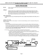
CAUTION:
Before servicing this chassis, it is important that the service person read the "SAFETY PRECAUTIONS" and
"PRODUCT SAFETY NOTICE" contained in this manual.
Ser
Ser
Ser
Ser
Service
vice
vice
vice
vice
Manual
Manual
Manual
Manual
Manual
2009
2009
2009
2009
2009
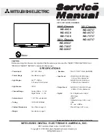
MITSUBISHI ELECTRIC
DLP PROJECTION HDTV
V41C, V41 & V41+ CHASSIS
• Speakers
:
Two 5½"x2¼" Oval
(8
Ω
10W)
• Input Level
: VIDEO IN JACK (RCA Type)
1.0Vp-p 75
Ω
unbalanced
: AUDIO IN JACK (RCA Type)
-4.7dBm 43k
Ω
unbalanced
• Output Level
: AUDIO OUT JACK (RCA Type)
-4.7dBm 4.7k
Ω
unbalanced
• Digital
: AC-3 Digital Audio Output
(RCA Type)
: HDMI
TM
:
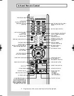
IR Blaster Output (V41+ only)
:
USB
: PC - use HMDI
TM \
:
Wired IR Input (V41+ only)
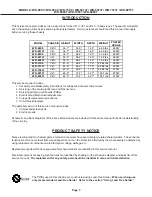
WD-52327
V41C Chassis
WD-60C9
WD-65C9
WD-73C9
WD-52527
Pb Solder
V41 Chassis
WD-60737
WD-65737
WD-73737
WD-82737
V41+ Chassis
WD-65837
WD-73837
WD-82837
SPECIFICATIONS
• Power Input
: AC 120V, 60Hz
•
Power Usage
: See table on page 5
• Light Engine
: DLP
TM
(1080p)
5 Primary Color System
• Light Source
: 180W
• Channel Range
: Analog Cable - 1~125
Digital Cable - 1~135
•
Antenna Input
: 1 RF 75
Ω
unbalanced
• Tuning
: 1 NTSC/ATSC/QAM
• Cabinet Dimensions
: See Table on page 5
• Weight
: See table on page 5
Summary of Contents for WD-60737
Page 2: ......