4-7
Parallel Outputs
Most of the parallel outputs are listed in
Table 4-2.
Most
of them have been used before and need no explana-
tion. However, the function of two items should be de-
scribed.
BWC (Band Width Control)
This line is directed to the Doubler circuitry, and auto-
matically becomes active when the signal source is
NTSC. The Doubler circuit is designed to produce the
best possible picture for an HDTV signal. Due to this
design, artifacts may appear in the picture when the sig-
nal source is NTSC.
With an NTSC source, the BWC line auto-
matically goes High. The High reduces some
of the high frequency output from the Dou-
bler, removing the unwanted artifacts.
BLK-EN
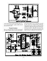
Figure 4-8
illustrates the BLK-EN circuitry.
The BLK-EN selects the path for the OSD
insertion timing signal (DM-BLK). The OSD
signals and the DM-BLK timing signal are
generated in the DM Module.
If the source signal is not from the DTV Tuner
or a 1394 input, the OSD signal is inserted
in the main signal in the VCJ IC2V01. The
Timing Signal (DM-BLK) is applied to the
inputs of IC2V02 and ICSVO3. IC2V02
directs the signal to the VCJ, and IC2V03 directs the
signal to the Doubler circuit. The path of the DM-BLK
signal is determined by BLK-EN from the TV µPC.
BLK-EN is applied directly to the OE (Output Enable)
input of IC2V03, and is inverted by Q2X04 and ap-
plied to the OE input of IC2V02. IC2V02 and IC2V03
are enabled when their OE input GOES Low.
When EN-BLK is High, IC2V02 is enabled and the
DM-BLK is directed to the VCJ. When EN-BLK is
Low, DM-BLK is directed to the Doubler. DM-BLK
is needed in Doubler, even though the OSD insertion
for a DM signal occurs in the DM Module.
Additional IC7A00 Outputs
Pin #
Name
Purpose
42
BLNK-CRT
Blanks CRTs during Input &Channel changes.
49
PON-2
Power ON: (Defl, Conv, HV, etc. circuitry)
50
PON-1
Power ON: Signal Processing circuitry)
51
BWC
Band Width Control for Doubler Output
52
F
Sets the Free Run Horizontal Frequency
56
F31K
Decreases H-Defl DC supply for 31.5 kHz.
57
DEFL-MUTE
Decreases H-Defl DC supply during freq. change.
71
BLK-EN
Enables OSD Insertion
76
MUTE SUB
Mutes Sub Picture Audio Output
80
MUTE SPKR
Mutes the TV's Speakers
82
POWERGOOD
Informs the DM that the DC Power is ok
86
MUTE MON
Mutes Monitor Out Audio
87
SUB POWER
Activates/Deactivates the Economy Mode
Table 4-2: µPC Outputs
Summary of Contents for WS-48513
Page 2: ......
Page 4: ......
Page 17: ...11 Figure 13 V23 Chassis DVI Input Block Diagram ...
Page 22: ...1 4 Figure 1 4 PCB Locations Figure 1 5 Main Component Locations ...
Page 40: ...3 10 ...
Page 70: ...8 2 Figure 8 2 Overall Sound Circuitry Block Diagram ...
Page 72: ...8 4 ...
Page 75: ......


