5-6
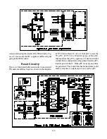
Monitor Out Circuit
Figure 5-5
shows that the Monitor Output signal source
is limited to an NTSC source, or the DM Module. The
NTSC Y and C signals from the 3DYC Comb Filter,
are directed back to IC2L00. IC2L00 directs the sig-
nals to the monitor Inputs of IC2K00. IC2K00 selects
the signal from IC2L00 or the DM signal input at pins
24 and 26 of IC2K00.
If the signal source is from a Component Input, the DTV
Input, VGA Input or MLINK Input, no signal is avail-
able at the Monitor Outputs.
Summary of Contents for WS-48513
Page 2: ......
Page 4: ......
Page 17: ...11 Figure 13 V23 Chassis DVI Input Block Diagram ...
Page 22: ...1 4 Figure 1 4 PCB Locations Figure 1 5 Main Component Locations ...
Page 40: ...3 10 ...
Page 70: ...8 2 Figure 8 2 Overall Sound Circuitry Block Diagram ...
Page 72: ...8 4 ...
Page 75: ......


