-
351
-
'12 • PAC-T-173
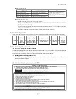
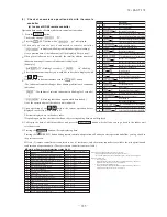
(c) Outdoor inverter PCB replacement procedure
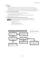
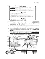
Precautions for Safety
• Since the following precaution is the important contents for safety, be sure to observe them.
WARNING and CAUTION are described as follows:
WARNING
Indicates an imminently hazardous situation which will result in death or serious
injury if proper safety procedures and instructions are not adhered to.
Indicates a potentially hazardous situation which may result in minor or moderate
injury if proper safety procedures and instructions are not adhered to.
CAUTION
WARNING
• Securely replace the PCB according to this procedure.
If the PCB is incorrectly replaced, it will cause an electric shock or fire.
• Be sure to check that the power source for the outdoor unit is turned OFF before replacing the
PCB. The PCB replacement under current-carrying will cause an electric shock or fire.
• After finishing the PCB replacement, check that wiring is correctly connected with the PCB before
power distribution. If the PCB is incorrectly replaced, it will cause an electric shock or fire.
CAUTION
• Band the wiring so as not to tense because it will cause an electric shock.
Replace the inverter PCB according to the following procedure.
㧍
㧍
㧍
㧍
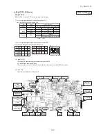
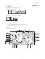
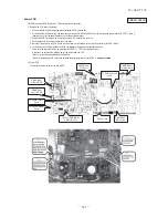
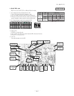
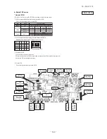
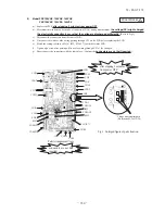
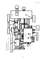
1) Model FDC71VNX
a) Replace the PCB
after elapsing 3 minutes from power OFF.
(
Be sure to measure voltage (DC)
between T26 and T27 on inverter PCB, and
check that the voltage is
discharged sufficiently (10V or less)
. (Refer to Fig.1))
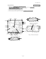
b) Take off the connection of inverter PCB terminal and connector, and remove the screw of power transistor (IC10),
active filter (IC2), and diode stack (DS1) then remove the PCB. Wipe off the silicon grease neatly on the controller’s
radiation heat fins. (Refer to Fig.1 and Parts arrangement view)
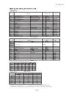
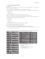
c) Refer to table1 for the setting of switch (JSW10, 11) of new PCB.
d)
Before installing the power transistor (IC10), active filter (IC2), and diode stack (DS1) on the new PCB, apply
silicon grease equally to the their surface. (Make full use of the silicon grease.)
They may be damaged unless
they apply it
.
e) Tighten the screw of power transistor (IC10), active filter (IC2), and diode stack (DS1) on inverter PCB and connect
terminal and connector. Confirm the connection and there is not the half insertion.
Tighten properly power
transistor, (IC10) active filter (IC2), and diode stack (DS1) with a screw and make sure there is no
slack. They can be damage if not properly tighten.
(Recommended tightening torque: power transistor
(IC10)1.2±0.1 and active filter (IC2)0.98±0.1, diode stack(DS1) 0.5±0.1 Unit N·m
-1
OFF
-1
ON
-2
OFF
-2
ON
-3
OFF
-3
O N
JSW10
-4
OFF
JSW11
-4
O N
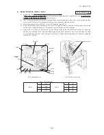
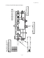
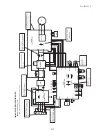
Parts arrangement view
Fig. 1 Position of fastontab and terminal
Table. 1 Switch setting
T24
(YELLOW)
CNI4
T27
(BLUE)
T25
(YELLOW)
T26
(RED)
T28 (RED)
CNG2
T22
(WHITE)
T21
(RED)
Voltage measurement point
(T26 (red), T27 (blue))
T30 (BLUE)
T29(WHITE)
Parts No.
JSW11
JSW10
CNI2
CNO1
SCREW OF POWER TRANSISTOR
(IC10)
SCREW OF DIODE STACK
(DS1)
SCREW OF ACTIVE FILTWER
(IC2)
after elapsing 3 minutes
from power OFF
Connectors are
not half inserted
PCA012D022G
B
Summary of Contents for FDC Series
Page 95: ... 94 12 PAC T 173 Models FDT100VF 125VF 140VF H H H H H C B A F G D G PJF000Z285 ...
Page 98: ... 97 12 PAC T 173 Models FDEN60VF 71VF C 2 C 1 A B A B D C 1 C 2 C 1 C 2 E G F B PFA003Z817 ...
Page 113: ... 112 12 PAC T 173 b Wireless remote controller RCN E1R 60 17 150 Unit mm ...
Page 278: ... 277 12 PAC T 173 ー K ...
Page 346: ... 345 12 PAC T 173 Power PCB 1BSU OVNCFS 4GRNCEG VJG 2 ...
Page 518: ... 517 12 PAC T 173 3 5 SUPER LINK E BOARD SC ADNA E F SL2NA E and SL3N AE BE to control ...
Page 519: ... 518 12 PAC T 173 ...

