


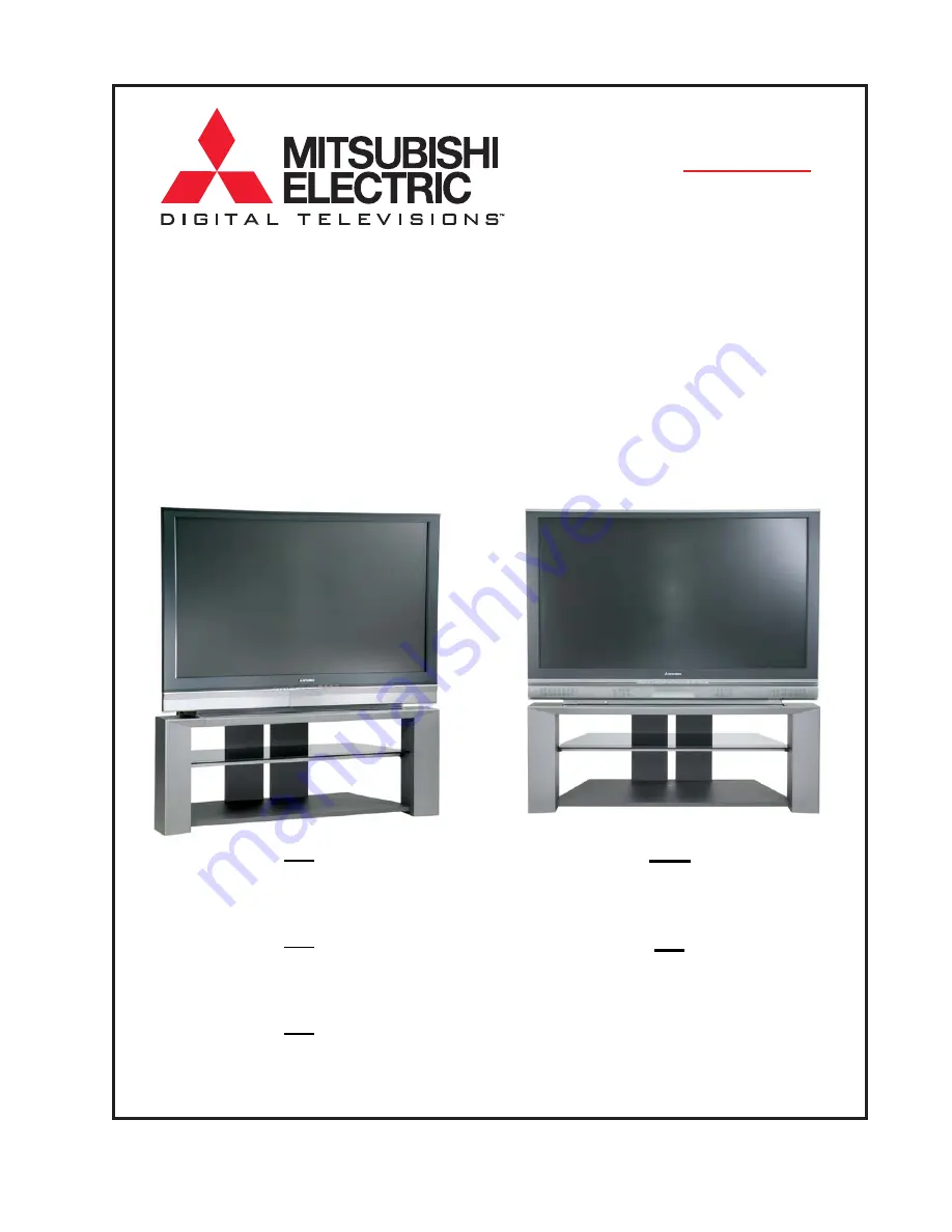
T
2005
2006
ECHNICAL
RAINING
Projection Television
Training Manual
Including…
Down-to-1
High Speed Troubleshooting
COPYRIGHT © 200
6
MITSUBISHI DIGITAL ELECTRONICS AMERICA, INC.
ALL RIGHTS RESERVED
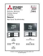
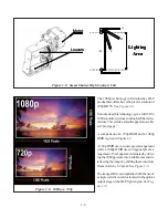
1080p
DLP™
720p
LCD
WD-52527 WD-62527
WD-52528 WD-62528
V28
V29
WD-52627
WD-62628
WD-52628 WD-62827 WD-73727
WD-62628
WD-73827
V31
WD-62927
WD-73927
V30
WD-52526 WD-62526
V28L
Summary of Contents for Mr.Slim WD-52627
Page 2: ......
Page 4: ...II...
Page 50: ...4 8...
Page 54: ...5 4 Figure 5 3A V28 PWB POWER DC to DC Supplies...
Page 55: ...5 5 Figure 5 3B DLP PWB POWER DC to DC Supplies...
Page 58: ...5 8 Figure 5 7 DLP Engine Power Supply Figure 5 8 Hard Disc HDD Power Supply V30 and V31 Only...
Page 59: ...5 9 Figure 5 9...
Page 60: ...5 10 Figure 5 10...
Page 63: ...5 13 Figure 5 13 Analog Video Signal Path...
Page 64: ...5 14 Figure 5 15 Video Record Path V30 and V31 only Figure 5 14 Analog Video Signal Path...
Page 69: ...5 19 Figure 5 22 DLP Engine Protect Circuitry Figure 5 23 Short Detection Circuitry...
Page 70: ...5 20...
Page 71: ......


