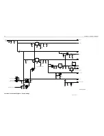
Controller Board Audio and Signalling Circuits
1-15
2.4.2
Audio Processing and Digital Volume Control
The receiver audio signal enters the controller section from the IF IC on DISC AUDIO. The signal is
DC coupled by R0228 and enters the ASFIC CMP via the DISC pin U0221-2.
Inside the ASFIC CMP, the signal goes through 2 paths in parallel, the audio path and the PL/DPL
path.
The audio path has a programmable amplifier, whose setting is based on the channel bandwidth
being received, then a LPF filter to remove any frequency components above 3000Hz and then an
HPF to strip off any sub-audible data below 300Hz. Next, the recovered audio passes through a de-
emphasis filter if it is enabled (to compensate for Pre-emphasis which is used to reduce the effects of
FM noise). The IC then passes the audio through the 8-bit programmable attenuator whose level is
set depending on the value of the volume control. Finally the filtered audio signal passes through an
output buffer within the ASFIC CMP. The audio signal exits the ASFIC CMP at pin AUDIO (U0221-
41).
The µP programs the attenuator, using the SPI BUS, based on the volume setting. The minimum /
maximum settings of the attenuator are set by codeplug parameters.
Since sub-audible signalling is summed with voice information on transmit, it must be separated from
the voice information before processing. Any sub-audible signalling enters the ASFIC CMP from the
IF IC at DISC U0221-2. Once inside it goes through the PL/DPL path. The signal first passes through
one of 2 low pass filters, either PL low pass filter or DPL/LST low pass filter. Either signal is then
filtered and goes through a limiter and exits the ASFIC CMP at LSIO (U0221-18). At this point the
signal will appear as a square wave version of the sub-audible signal which the radio received. The
microprocessor U0101-80 will decode the signal directly to determine if it is the tone / code which is
currently active on that mode.
2.4.3
Audio Amplification Speaker (+) Speaker (-)
The output of the ASFIC CMP’s digital volume pot, U0221-41 is routed through dc blocking capacitor
C0265 to a buffer formed by U0211-1. Resistors R0265 and R0268 set the correct input level to the
audio PA (U0271). This is necessary because the gain of the audio PA is 46 dB, and the ASFIC CMP
output is capable of overdriving the PA unless the maximum volume is limited. Resistor R0267 and
capacitor C0267 increase frequency components below 350 Hz.
The audio then passes through R0269 and C0272 which provides AC coupling and low frequency
roll-off. C0273 provides high frequency roll-off as the audio signal is routed to pins 1 and 9 of the
audio power amplifier U0271.
The audio power amplifier has one inverted and one non-inverted output that produces the
differential audio output SPK+ / SPK- (U0271-4/6). The inputs for each of these amplifiers are pins 1
and 9 respectively; these inputs are both tied to the received audio. The audio PA’s DC biases are
not activated until the audio PA is enabled at pin 8.
The audio PA is enabled via the ASFIC CMP (U0221-38). When the base of Q0271 is low, the
transistor is off and U0271-8 is high, using pull up resistor R0273, and the Audio PA is ON. The
voltage at U0273-8 must be above 8.5VDC to properly enable the device. If the voltage is between
3.3 and 6.4V, the device will be active but has its input (U0273-1/9) off. This is a mute condition
which is used to prevent an audio pop when the PA is enabled.
The SPK+ and SPK- outputs of the audio PA have a DC bias which varies proportionately with FLT
A+ (U0271-7). FLT A+ of 11V yields a DC offset of 5V, and FLT A+ of 17V yields a DC offset of 8.5V.
If either of these lines is shorted to ground, it is possible that the audio PA will be damaged. SPK+
and SPK- are routed to the accessory connector (J0501-16 and 1) and to the controlhead (connector
J0401-2 and 3).
Summary of Contents for 6864115B62-C
Page 1: ...Professional Radio GM Series Detailed Service Manual 6864115B62 C ...
Page 2: ...ii ...
Page 4: ...iv ...
Page 5: ...Professional Radio GM Series Service Maintainability Issue July 2007 ...
Page 8: ...ii ...
Page 22: ...2 10 MAINTENANCE ...
Page 25: ...Professional Radio GM Series Controlhead Service Information Issue July 2007 ...
Page 77: ...Professional Radio GM Series Controller Service Information Issue May 2007 ...
Page 100: ...2 2 TROUBLESHOOTING CHARTS ...
Page 104: ...3 4 Controller schematics parts list ...
Page 154: ...3 52 Controller T12 Schematic Diagrams ...
Page 155: ...Professional Radio GM Series VHF 136 174MHz Service Information Issue May 2007 ...
Page 164: ...1 6 MODEL CHART AND TECHNICAL SPECIFICATIONS ...
Page 176: ...2 12 THEORY OF OPERATION ...
Page 186: ...3 10 TROUBLESHOOTING CHARTS ...
Page 190: ...4 4 VHF PCB SCHEMATICS PARTS LISTS ...
Page 252: ...4 66 VHF 1 25W PCB 8471235L02 Schematics VHF 136 174 MHz IF ...
Page 256: ...4 70 VHF 1 25W PCB 8471235L02 Schematics ...
Page 257: ...Professional Radio GM Series UHF 403 470MHz Service Information Issue May 2007 ...
Page 266: ...1 6 MODEL CHART AND TECHNICAL SPECIFICATIONS ...
Page 366: ...2 12 THEORY OF OPERATION ...
Page 372: ...3 6 Low Band TROUBLESHOOTING CHARTS ...

