HC05A24EM USER’S MANUAL
MOTOROLA
3-6
3
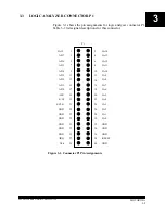
Table 3-1.
Logic Analyzer Connector P1 Signal Descriptions
Pin Number
Signal Mnemonic
Signal Name and Description
3, 5, 7, 9, 11, 13,
15, 17
AD7-AD0
Data bus:- MCU bidirectional data bus.
1, 2, 4, 6, 8, 10, 12,
14, 16, 18, 20, 22,
24, 26, 28, 30
LA15-LA0
Address bus:- MCU output address bus.
19
/LIR
Load Instruction Register:- Active-low output
signal, asserted when an instruction starts.
21
R/W
Read/Write:- Output signal that indicates the
direction of data transfer.
37
/IRQ
MCU Interrupt Request:- Active-low input sig-
nal from the target that asynchronously applied
an MCU interrupt.
38
/RESET
Reset:- Active-low bidirectional signal for start-
ing an EVS reset.
23
ECLK
E-clock:- Internally generated output clock sig-
nal used as a timing reference.
25, 27, 29, 31, 32,
33, 34, 35, 36, 40
GND
Ground
39
Vdd
+5Vdc power:- Input voltage (+5Vdc @
1A(max)) used by the EVS logic circuits.


