background image

HC05A24EM USER’S MANUAL

MOTOROLA
1-4

1

1.3

TARGET CONNECTORS AND CABLE INFORMATION

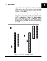
Figure 1-2 and 1-3 show the pin assignments for connectors P7 and P8.
For signal descriptions, consult the technical data book for the
M68HC05A24 MCU.

As connector P1 has more importance to an HC05EVS than to an
MMDS05, pin assignments for connector P1 are in Chapter 3.

To configure your A24EM for use as part of an MMDS05, follow the
instructions of Chapter 2. To configure your A24EM as part of an
HC05EVS, follow the instructions of Chapter 3.

2

4

6

8

10

12

14

16

18

20

22

24

26

28

30

32

34

36

38

40

PWM

1

3

 5

7

9

11

13

15

17

19

21

23

25

27

29

31

33

35

37

39

P7

 GND

/RESET

AD0

AD1

VDD

GND

GND

IRQ2

/IRQ

GND

PA5

PA4

PA2

PA0

PC6

PC4

PC2

PC0

GND

GND

GND

GND

GND

GND

GND

GND

GND

/IRQ1

PA7

PA6

GND

PA3

PA1

PC3

PC1

GND

GND

Figure 1-2. Connector P7 Pin Assignments

PC7

PC5

Summary of Contents for A24EM

Page 1: ...MOTOROLA SEMICONDUCTOR USER S MANUAL c MOTOROLA INC 1994 All Rights Reserved HC05A24EMUM D July 1996 HC05A24 EMULATOR MODULE USER S MANUAL First Edition ...

Page 2: ...duct could create a situation where personal injury or death may occur Should buyer purchase or use Motorola products for any such unin tended or unauthorized application Buyer shall indemnify and hold Motorola and its officers employees subsidiaries affiliates and distributors harmless against all claims costs damages and expanses and reasonable attorney fees arising out of directly or indirectly...

Page 3: ...Header P4 2 2 2 1 2 COP Disable Header P5 2 2 2 1 3 Clock Source Select Header P6 2 3 2 1 4 Clock Divider Header P9 2 3 2 2 Installing Personality And Help Files 2 4 2 2 1 Personality File 2 4 2 2 2 Help File 2 4 2 3 Remaining System Installation 2 5 CHAPTER 3 HC05EVS CONFIGURATION AND OPERATION 3 1 3 1 Setting A24EM Jumper Headers 3 1 3 1 1 Reset Select Header P4 3 1 3 1 2 COP Disable Header P5 3...

Page 4: ... 3 1 2 Connector P7 Pin Assignment 1 4 1 3 Connector P8 Pin Assignment 1 5 1 4 Target Cable and Head Assembly 1 7 3 1 Connector P1 Pin Assignment 3 5 TABLES Table Page 1 1 Parts required to form a target cable assemble for A24EM 1 6 3 1 Logic Analyzer Connector P1 Signal Descriptions 3 6 ...

Page 5: ...nclosure containing the control board and the internal power supply Most system cables connect to the MMDS05 station module The cable to an optional target system however runs through an aperture in the station mod ule enclosure to connect directly to the emulator module an emulator module EM such as the A24EM a printed circuit board that enables system functionality for a specific MCU The EM fits...

Page 6: ... PFB the bottom board which supports the emulator module The platform board has connectors for power and for the terminal or host computer an emulator module EM such as the A24EM a printed circuit board that enables system functionality for a specific MCU The EM fits onto the PFB The EM has connectors for a target cable and a cable to a logic analyzer an RS 232 serial cable the cable that connects...

Page 7: ...for a 56 pin SDIP cable assembly purchased separately from the A24EM provide an interface to your target system If you install the A24EM in the MMDS05 station module the target cable passes through the slit in the station module enclosure Connector P1 connects to a logic analyzer Connector P1 has more significance for an EVS system as an MMDS05 system includes a bus analyzer Expansion header conne...

Page 8: ...connector P1 are in Chapter 3 To configure your A24EM for use as part of an MMDS05 follow the instructions of Chapter 2 To configure your A24EM as part of an HC05EVS follow the instructions of Chapter 3 2 4 6 8 10 12 14 16 18 20 22 24 26 28 30 32 34 36 38 40 PWM 1 3 5 7 9 11 13 15 17 19 21 23 25 27 29 31 33 35 37 39 P7 GND RESET AD0 AD1 VDD GND GND IRQ2 IRQ GND PA5 PA4 PA2 PA0 PC6 PC4 PC2 PC0 GND ...

Page 9: ...2 34 36 38 40 GND 1 3 5 7 9 11 13 15 17 19 21 23 27 29 31 33 35 37 39 P8 TCAP TCMP1 HRX HTX GND HTX_CLK PF4 PF3 PF1 PB7 PB5 PB3 PB1 GND PE7 PE6 PE5 PE3 PE1 PE0 GND GND GND HRX_CLK PF5 GND PF2 PF0 PB6 PB4 PB2 PB0 GND GND GND PE4 PE2 GND GND Figure 1 3 Connector P8 Pin Assignments 25 ...

Page 10: ...ssembly for the A24EM To use a SDIP target cable connect the large cable terminator of M68CLB05B to M68TB05A24B56 They should be connected in such a way that the arrow marked on the target head is pointing to the target cable Next connect the small cable terminator to the A24EM target connectors P7 and P8 The connector at the far end of the cable should be connected to P7 and the other to P8 Plug ...

Page 11: ...4EM USER S MANUAL MOTOROLA 1 7 1 Target Cable Emulator Terminator Head Terminator connects to target head Target Head Connects to EM target conectors Plugs to target system MCU socket or surface mount adapter ...

Page 12: ...ph 2 2 explains how to install personality and help files pertaining to the A24EM Paragraph 2 3 explains remaining system installation Note that you can configure an A24EM already installed in the MMDS05 station module enclosure To do so switch off station module power remove the hatch then follow the guidance of this chapter CAUTION Be sure to switch off power if you reconfigure an installed EM R...

Page 13: ...ration would interfere with correct operation of the RESETIN and RESETOUT commands 2 1 2 COP Disable Header P5 Jumper header P5 allows the user to enable disable the internal COP during software development The diagram below shows the factory configuration the fabricated jumper between pins 1 and 2 enables the internal COP To disable it remove the fabricated jumper between pins 1 and 2 The jumper ...

Page 14: ...e MMDS05 OSC command to select a frequency 2 1 4 Clock Divider Header P9 Jumper header P9 determines which internal clock divider of the MCU to use on power up or reset The diagram below shows the factory con figuration the fabricated jumper between pins 1 and 2 selects the divide by two MCU clock divider This is the correct configuration for a 4 MHz clock source If a 16 MHz clock source is used T...

Page 15: ...tte to a hard disk Personality files are usually installed in the directory from which the MMDS05 software is executed If a personality file is not located in that directory the MMDS05 software displays a window with which the user can search the directory structure to find the correct file More than one personality file can be installed the MMDS05 operating software automatically loads the person...

Page 16: ...ectors P2 and P3 on the bottom of the board and control board connectors P11 and P12 Snap the mounting holes of the EM onto the plastic standoffs Connect the target cable if appropriate Replace the panel If your A24EM already is installed in the station module reconnect the target cable if necessary Replace the panel At this point you are ready to make remaining cable connections as necessary and ...

Page 17: ...HC05A24EM USER S MANUAL MOTOROLA 2 6 2 ...

Page 18: ...ng the A24EM in an HC05EVS Paragraph 3 3 explains pin assignments and signal descriptions for the logic analyzer connector P1 Paragraph 3 4 explains remaining system configuration Note that you can configure an A24EM already installed on the HC05EVS platform board To do so disconnect platform board power then follow the guidance of this chapter CAUTION Be sure to disconnect power if you reconfigur...

Page 19: ...and Insert a fabricated jumper into platform board header J3 3 1 2 COP Disable Header P5 Jumper header P5 allows the user to enable disable the internal COP during software development The diagram below shows the factory configuration the fabricated jumper between pins 1 and 2 enables the internal COP To disable it remove the fabricated jumper between pins 1 and 2 The jumper setting is sampled onc...

Page 20: ...24EM that is part of an HC05EVS system 3 1 4 Clock Divider Header P9 Jumper header P9 determines which internal clock divider of the MCU to use after power on or reset The diagram below shows the factory con figuration the fabricated jumper between pins 1 and 2 selects the divide by two MCU clock divider This is the correct configuration for a 4 MHz clock source If a 16 MHz clock source is used Th...

Page 21: ...never would execute the instruction However it would appear to you that the instruction had executed You may enter a G command while the PC points to this type of instruction as long as the instruction is not a breakpoint address Limitation 3 IRQ SWI Whenever possible avoid mixing interrupt requests IRQs and user software interrupts SWIs This prevents a possible IRQ SWI timing problem a concurrent...

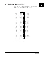
Page 22: ...gnal descriptions for this connector 2 4 6 8 10 12 14 16 18 20 22 24 26 28 30 32 34 36 38 40 LA12 LA11 LA10 LA9 LA8 LA7 LA6 LA5 LA4 LA3 LA2 LA1 LA0 GND 1 3 5 7 9 11 13 15 17 19 21 23 25 27 29 31 33 35 37 39 AD7 AD6 AD5 AD4 AD3 AD2 AD1 AD0 LIR R W ECLK Figure 3 1 Connector P1 Pin Assignments P1 GND IRQ Vdd LA13 LA14 LA15 GND GND RESET GND GND GND GND GND GND ...

Page 23: ...ster Active low output signal asserted when an instruction starts 21 R W Read Write Output signal that indicates the direction of data transfer 37 IRQ MCU Interrupt Request Active low input sig nal from the target that asynchronously applied an MCU interrupt 38 RESET Reset Active low bidirectional signal for start ing an EVS reset 23 ECLK E clock Internally generated output clock sig nal used as a...

Page 24: ...program for driving the A24EM the orignal Eprom must be reinserted into U2 if the user decides to use another EM to emulate an MCU of a different series Next find jumper header J1 of the HC05EVS platform board Make sure that four fabricated jumpers are installed per the diagram below To install the A24EM on an HC05EVS platform fit together EM con nectors P2 and P3 on the bottom of the board and pl...

Reviews: