Theory of Operation:
Transceiver Board
3-27
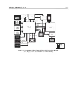
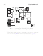
3.1.4.9 Buffers and VCOs
Q774 and surrounding circuitry is the prescalar buffer that takes the output of the VCOs and feeds
the prescalar input to the Trident IC, pin G1 (M_PRSC).
Q713 and surrounding circuitry is a buffer that provides the correct drive level to the receiver section
(via the transmission line TL_RX_LO) and to the input to the TX buffer (Q842 and surrounding
circuitry). Q712 and surrounding circuitry provide the bias to the buffer. The buffer formed by Q713
and its associated circuitry is called a "pre-buffer" at this stage.
R712, R713 and R714 help provide some extra isolation to the receiver.
Q842 and surrounding circuitry is the transmit injection buffer. The transmit injection buffer provide
the correct drive level to the transmitter section (via the transmission line TL_TX_LO). Q703 and
surrounding circuitry provide the bias to the transmit injection buffer.
VHF:
The TX and RX VCOs used for the VHF band are contained in Y704 and Y707 respectively. To
select the VHF TX VCO, pin 3 (SEL1) must be at a high logic level and pin 5 (SEL2) at a low logic
level, on Y704. The VHF TX output of Y704, pin 1 (POUT) goes to pin 4 (RF1) of U708. The output of
U708, pin 1 (RFC), then goes to pin 4 (RF1) of U709. The output of U709, pin 1 (RFC), is then split
into two signals. One to the prescalar buffer input and the other to the pre-buffer. The output of the
prebuffer is then fed to pin 1 (RFC) of U710. The VHF TX signal then goes to the divide-by-two
circuitry in the Trident IC, pin J2 (ESC_IN). Resistors R703, R704 and capacitors C705, C748 and
C747 provide the correct bias for the divide-by-two output. The output of the divide-by-two circuitry,
pin K1 (ESCD2_OUT) then goes through a 'second harmonic filter' (comprised of C800, C801, C803
and L802) and attenuator (comprised of R709, R710 and R711). The output of the attenuator goes to
pin 8 (RF3) of U711. The output of U711, pin 1 (RFC) is then fed to the transmit buffer (Q842 and
surrounding circuitry). The output of the transmit injection buffer, then goes to the transmit section via
the TL_TX_LO transmission line.
To select the VHF RX VCO, pin 3 (SEL1) must be at a high logic level and pin 5 (SEL2) at a low logic
level, on Y707. The output of the VHF RX VCO, pin 1 (POUT) of Y707 goes to pin 8 (RF3) of U709.
The output of U709, pin 1 (RFC) is split into two signals, one to the prescalar buffer (Q774) and the
other to the pre-buffer. The output of the pre-buffer is then fed to pin 1 (RFC) of U710. The output of
U710, pin 5 (RF2) then goes to the attenuator (comprised of R712, R713 and R714) and then fed to
the receiver section via the TL_RX_LO transmission line.
UHF1:
The TX and RX VCOs used for UHF1 are contained in Y705 and Y704. To select the UHF RX
VCO from (380–450 MHz), pin 3 (SEL1) must be at a high logic level and pin 5 (SEL 2) at a low logic
level, on Y704. To select UHF RX VCO (450–470 MHz), pin 3 (SEL1) must be at a low logic level and
pin 5 (SEL 2) at a high logic level, on Y704. The UHF RX VCO output of Y704, pin 1 (POUT), is then
fed to pin 4 (RF1) of switch U708. The output of U708, pin 1 (RFC), then goes to pin 4 (RF1) of
U709. The output of U709, pin 1 (RFC), is then split into two signals. One to the prescalar buffer
input and the other to the pre-buffer. The output of the prebuffer is then fed to pin 1 (RFC) of U710.
The output of U710, pin 5 (RF2) then goes to the receiver section via TL_RX_LO transmission line.
To select the UHF TX VCO (380–445 MHz), pin 3 (SEL1) must be at a high logic level and pin 5
(SEL2) at a low logic level, on Y705. To select the UHF TX VCO (445–470 MHz), pin 3 (SEL1) must
be at a low logic level and pin 5 (SEL2) at a high logic level, on Y705. The UHF TX VCO output of
Y705, pin 1 (POUT), is then fed to pin 5 (RF2) of switch U708. The output of U708, pin 1 (RFC), then
goes to pin 4 (RF1) of U709. The output of U709, pin 1 (RFC), is then split into two signals. One to
the prescalar buffer input and the other to the prebuffer. The output of the prebuffer is then fed to pin
1 (RFC) of U710. The output of U710, pin 4 (RF1) then goes to pin 4 (RF1) of U711. The output of
U711, pin 1 (RFC) then goes to the transmit injection buffer (comprised of Q842 and surrounding
circuitry). The output of the transmit injection buffer, then goes to the transmit section via the
TL_TX_LO transmission line.
Summary of Contents for ASTRO APX 7000
Page 1: ......
Page 4: ...iv Document History Notes ...
Page 24: ...2 4 Radio Power DC Power Routing VOCON Board Notes ...
Page 98: ...3 74 Theory of Operation Global Positioning System GPS ...
Page 163: ...Troubleshooting Charts PA Failure 5 59 ...
Page 164: ...5 60 Troubleshooting Charts PA Failure ...
Page 276: ...7 58 Troubleshooting Tables List of Board and IC Signals Notes ...
Page 318: ...8 42 Schematics Boards Overlays and Parts Lists Transceiver RF Boards VHF 700 800 Notes ...
Page 380: ...8 104 Schematics Boards Overlays and Parts Lists Transceiver RF Boards UHF1 700 800 MHz Notes ...
Page 432: ...8 156 Schematics Boards Overlays and Parts Lists Transceiver RF Boards UHF1 VHF Notes ...
Page 458: ...8 182 Schematics Boards Overlays and Parts Lists Transceiver RF Boards UHF1 UHF2 Notes ...
Page 498: ...8 222 Schematics Boards Overlays and Parts Lists Transceiver RF Boards UHF2 700 800 MHz Notes ...
Page 546: ...8 270 Schematics Boards Overlays and Parts Lists Transceiver RF Boards UHF2 VHF Notes ...
Page 606: ...8 330 Schematics Boards Overlays and Parts Lists VOCON Boards Notes ...
Page 638: ...Glossary 10 Glossary Notes ...
Page 643: ......


