6881094C31-E
November 16, 2006
Theory of Operation:
Transceiver Board
3-9
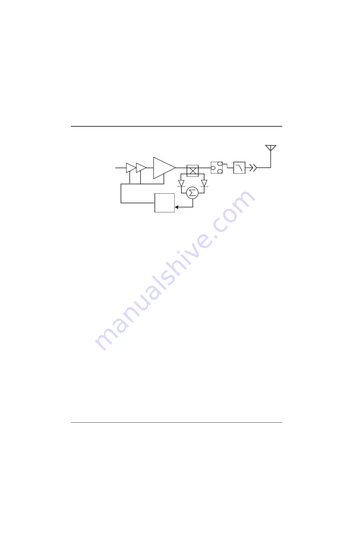
Figure 3-6. Transmitter Block Diagram
3.1.3.1 Power Distribution
To minimize voltage drop to the power amplifiers, net RAWB+ connects to power module Q107 and
the second stage of driver amplifier U102 through components having minimal series resistance—
ferrite beads and chokes only. During receive, no RF or DC bias is applied, and leakage current
through U102 and Q107 is less than 100 microamps. The first stage of U102 uses less than 50 mA
and is supplied by TX7V, which is switched on during TX, and switched off during RX or whenever
TXINH, the transmitter inhibit control line, is high.
VHF:
At a transmitter power of 6 Watts, the radio consumes approximately 2000 mA. Bias TX7V is
controlled by transistors Q101, Q102, Q103, and Q106.
UHF Range 1 and Range 2:
At the rated transmitter power of 5 Watts, the radio consumes
approximately 2000 mA. Bias TX7V is controlled by transistors Q101, Q102, Q103, and Q106.
700–800 MHz:
At a transmitter power of 3 Watts, the radio consumes approximately 1200 mA. Bias
TX7V is controlled by transistors Q101, Q102, Q103, and Q107.
3.1.3.2 Driver Amplifier
The driver amplifier IC (U102) contains two LDMOS FET amplifier stages and two internal resistor
bias networks. Pin 16 is the RF input. Modulated RF from the FGU, at a level of +3 dBm ±2 dB, is
coupled through a blocking capacitor to the gate of FET-1. An LC interstage matching network
connects the first stage output VD1 to the second stage input G2. The RF output from the drain of
FET-2 is pin 6 (RFOUT1). Gain control is provided by a voltage applied to pin 1 (VCNTRL). Typical
output power is about +27 dBm (500 mW) with VCNTRL at 5.0 V.
VHF:
L109 and C113 are the interstage matching network. Components C108–C111 and L106–L107
match the output impedance to maximize power transfer to Q107; capacitor C107 is a DC block.
UHF Range 2:
L109 and C113 are the interstage matching network. Components C108–C111 and
L105, L107, and L108 match the output impedance to maximize power transfer to Q107.
UHF Range 1 and 700–800 MHz:
L109 and C116 are the interstage matching network. Components
L105 and C110 match the output impedance to 50 ohms; capacitor C107 is a DC block.
Modulated RF
from FGU
Driver
amplifier
Power
amplifier
Directional
coupler
Antenna
switch
Harmonic
filter
Antenna
Forward and reverse power detectors
Vd = m*sqrt(P) + b
Summing
amplifier
RFIN
INT
PCIC
MAEPF-27408-O
Summary of Contents for ASTRO XTS-5000
Page 7: ...vi Table of Contents November 16 2006 6881094C31 E Notes ...
Page 11: ...x List of Figures November 16 2006 6881094C31 E Notes ...
Page 17: ...November 16 2006 6881094C31 E xvi CommercialWarranty Notes ...
Page 31: ...November 16 2006 6881094C31 E xxx Portable Radio Model Numbering System Notes ...
Page 83: ...November 16 2006 6881094C31 E 3 44 Theory of Operation Encryption Module ...
Page 135: ...November 16 2006 6881094C31 E 5 44 Troubleshooting Charts Secure Hardware Failure Notes ...
Page 175: ...November 16 2006 6881094C31 E 7 32 Troubleshooting Tables List of Board and IC Signals Notes ...
Page 367: ...November 16 2006 6881094C31 E Glossary 10 Notes ...
Page 373: ...Index 6 November 16 2006 6881094C31 E Notes ...


