May 28, 2008
6871620L01-C
3-10
Theory of Operation:
Transceiver Section
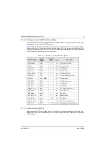
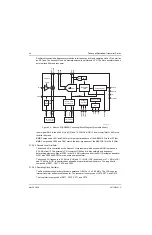
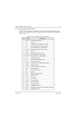
3.1.3.6.1 Power and Control
Since U104 is powered from switched B+, it makes its own regulated 4.5 Vdc to power the internal
logic. The supply input is V5EXT at pin 17, and the output is V45 at pin 16. RX at pin 23 is the control
signal to the antenna switch control circuit.
3.1.3.6.2 Voltage Multiplier
The PCIC contains an internal voltage multiplier. This multiplier produces signal V10 (pin 14), a 10-V
supply for the PCIC D/A converters (DACs). This enables the DACs outputs to reach 8 V. The FREF
signal is a 2.1 MHz clock used to switch the multiplier. The voltage multiplier is not used in the radio.
3.1.3.6.3 Automatic Level Control (ALC)
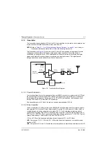
In TX mode, the PCIC disables the receiver, turns on the transmitter, and controls the TX power
level. The automatic level control (ALC) circuit operates as follows:
The power level is set by programming an internal DAC to a calibrated reference voltage. D/A
settings for the power set points were determined during radio tuning and stored in Flash ROM. An
internal op-amp compares the D/A reference voltage to the detector voltage at pin 1(RFIN) and
produces an error signal output. This signal is buffered by another op-amp, configured as a low-pass
filter, or integrator, to produce the INT output at pin 4 (TP104). This signal drives the base of voltage
follower Q101.
Transistor Q101 supplies current to drive the gain control pins of amplifiers U102 and Q107.
Resistors R105 and R106 determine the voltage ratio between U102 pin 2 (VCNTRL) and the Q107
gate. Transient response during key-up and key-down is controlled by the power amplifier rise and
fall times. External capacitors at pins CI, CJ, and CL, along with internal programmable resistors,
determine the ALC time constants.
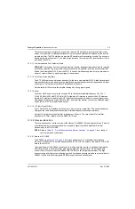
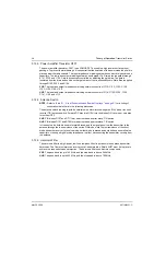
3.1.3.6.4 Temperature Cut Back
The PCIC contains a temperature cut-back circuit to protect the power amplifier (PA) from thermal
damage that might result from incorrect assembly of the radio. External sensor U103 is a linear
temperature-to-voltage transducer, placed near the hottest spot in the radio: power module Q107.
The output is a DC voltage at pin 2 (VOUT) proportional to the temperature at pin 3 (GND). VOUT is
750 mV at 25°C and increases by 10 mV/°C. The PCIC temperature cut-back threshold is
programmed to correspond to 85 or 90°C. Above this threshold, the ALC gradually cuts back the
transmitter until it is fully turned off at 110°C. The slope of cut-back versus temperature is set by
external resistor R111. Diode D104 clamps TEMP to a voltage not much less than VG (pin 15), about
1.3 V, to improve the transient response of the cut-back circuit. A secondary temperature cut back
circuitry is also included for enhanced thermal protection due to the small form factor of the radio.
Q102 along with RT150 and the surrounding support circuitry realizes the circuit. This extra
protection acts independently of the cut-back circuit within the PCIC and ensures the radio's
conformance to thermal safety limits.
3.1.3.6.5 D/A Outputs
In RX mode, the PCIC shuts down the transmitter, turns on the receiver, and tunes the RX front-end
pre-selector filters.
Signal VAR2 supplies the voltage used to tune both front-end pre-selector and post-selector filters.
The voltage range varies from 0.8 V to 2.2 V across the VHF band.
Summary of Contents for ASTRO XTSTM 4000
Page 1: ...COLOR CHORDS 7 ASTRO XTSTM 4000 Portable Radio Detailed Service Manual ...
Page 2: ......
Page 16: ...May 28 2008 6871620L01 C xiv Commercial Warranty Notes ...
Page 22: ...May 28 2008 6871620L01 C 1 6 Introduction Notes ...
Page 26: ...May 28 2008 6871620L01 C 2 4 Radio Power Notes ...
Page 56: ...May 28 2008 6871620L01 C 3 30 Theory of Operation Notes ...
Page 100: ...May 28 2008 6871620L01 C 6 8 Troubleshooting Waveforms Notes ...
Page 194: ...May 28 2008 6871620L01 C B 2 Motorola Service Centers Notes ...
Page 204: ...May 28 2008 6871620L01 C Glossary 10 Glossary Notes ...
Page 209: ......


