background image

2/6/98

Issue 1.0

25

Disassembly

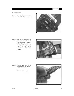
Flip Removal

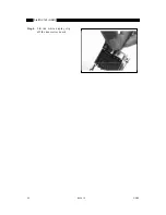
Step 1.

Using a dental pick, remove
the adhesive strip off the
base of the flip.

Step 2. Using tweezers, press the

hinge pin button in and over
toward the middle of the
flip.

Also, move the hinge pin
section above the button
toward the middle of the
flip.

Note: When reassembling
the flip, the button will click
back into place.

Remove the flip by pulling
up on the hinge pin side and
out on the other side.

The hinge shaft may come
loose from the flip.

Summary of Contents for cd 160

Page 1: ...StarTAC 160 GSM Cellular Subscriber Sector The World s Leading Cellular Telephone Manufacturer Service Manual Issue 1 0 ...

Page 2: ...y 5 Degrees RMS 20 Degrees peak Duplex Spacing 45 MHz Frequency Stability 0 10 ppm of the downlink frequency Rx Operating Voltage 3 0V dc to 5 1V dc battery 4 4V dc to 6 5V dc external connector Transmit Current 200 mA average 1 0 A peak Stand by Current Average 10mA DRX 2 Dimensions 98 3 mm L x 57 3 mm W x 22 5 mm D Size Volume 100 cubic cm Weight Approximately 99 5 g Includes Slim LiIon battery ...

Page 3: ...ate 100 k bits 2 Channel Hop Time 500 microseconds Time to Camp Approximately 10 seconds Table 4 Speech Coding Function Specification Speech Coding Type Regular Pulse Excitation Linear Predictive Coding with Long Term Prediction RPE LPC with LTP Bit Rate 13 0 k bps Frame Duration 20 ms Block Length 260 bits Classes Class 1 bits 182 bits Class 2 bits 78 bits Bit Rate with FEC Encoding 22 8 k bps Ta...

Page 4: ...ellular products Orders for all parts should be sent to the Motorola International Logis tics Department at the following address Attn Global Spare Parts Department Motorola Cellular Subscriber Group 2001 N Division St Harvard IL 60033 3674 U S A FAX 1 815 884 8354 When ordering replacement parts or equipment information the complete identi fication number should be included This applies to all co...

Page 5: ...option and the portable radiotele phone are connected to the vehicle electrical system as this may cause serious damage to the radio Disconnect the radio by removing the cable kit fuses DO NOT operate this equipment near elec trical blasting caps or in an explosive atmo sphere Mobile telephones are under certain conditions capable of interfering with blasting operations When in the vicinity of con...

Page 6: ...rity 7 Transceiver Labelling 7 Mini SIM CARDS 8 Testing 11 Verification 11 Manual Test Mode 12 Personality Transfer 15 Introduction 15 Normal Transfer 15 Master Transfer 16 Master SIM Card Creation 17 Disassembly 19 Introduction 19 Recommended Tools 19 Transceiver Disassembly 19 Troubleshooting 27 Introduction 27 Troubleshooting And Repair 27 Testing After Repair 27 Troubleshooting Supplements 33 ...

Page 7: ...viii Issue 1 0 2 6 98 StarTAC 160 GSM ...

Page 8: ...lightest battery The transceiver circuitry is contained on two multi layer boards the RF Logic board and the keyboard assembly The RF Logic board houses the RF and Audio Logic circuitry on separate sides in addition to SIM contacts the alert a 16 posi tion ZIF connector the microphone and an external connector The keyboard assembly houses the display reed switch and keyboard LEDs Electrical connec...

Page 9: ...2 Issue 1 0 2 6 98 StarTAC 160 GSM ...

Page 10: ...ly simplified and does not illustrate the full operating capabili ties techniques or technology incorpo rated in the system Using this technique radiation on a given channel is virtually contained in the cell operating on that channel and to some extent those cells directly adjacent to that cell Since the coverage area of a cell on a given channel is limited to a small area relative to the total s...

Page 11: ...resume that cell A operates on channels arbitrarily numbered 1 through 8 cell B operates on channels 9 through 16 cell C operates on channels 17 through 24 and cell D operates on channels 1 through 8 repeating the usage of those channels used by cell A In this system subscribers in cell A and subscribers in cell D could simulta neously operate on channels 1 through 8 The implementation of frequenc...

Page 12: ... the subscriber s distance from the base station As the radiotelephone moves from cell to cell its control is handed from one base station to another in the new cell This change is handled by the radiotele phone and base stations and is completely transparent to the user Service Area The area within which calls can be placed and received is defined by the system opera tors Because this is a radio ...

Page 13: ...6 Issue 1 0 2 6 98 StarTAC 160 GSM ...

Page 14: ...he units IMEI will change therefore the units label ling should be updated with the new IMEI An IMEI uniquely identifies a mobile station equipment to the system and is divided into the sections shown below Figure 4 IMEI Configuration REV S H This configuration consists of two blocks of two digits and denotes the software and hardware versions within the unit The first two digits correspond to the...

Page 15: ...ys away fron the phone The User Guide contains full information about inserting and removing the Mini SIM card Security Information To stop unauthorized personnel using your Mini SIM card the option of using a Personal Identity Number PIN is available When enabled the option requires on power up a verification number to be entered via the unit s keypad before the card can be used Three attempts to...

Page 16: ... is avail able When enabled this function requires that a three or four digit unlock code be entered via the units keypad before normal operation of the transceiver can take place The lock code can be changed by entering a set key sequence Further information on set key sequences can be derived from the unit s User Guide ...

Page 17: ...10 Issue 1 0 2 6 98 StarTAC 160 GSM ...

Page 18: ...to the slot at the side of the personal cellular telephone If required further information on Mini SIM card insertion is available on page 8 The telephone s antenna should now be removed see Disassembly on page 19 for further details When the antenna has been removed attach the antenna adaptor to the unit Slide a charged battery on to the back of the personal telephone so that the telephone can be...

Page 19: ...sue 1 0 2 6 98 StarTAC 160 GSM Figure 6 Testing Configuration Test Adaptor SKN4683A or SKN4665A Plugs into accessory connector of phone Unit To Be Tested GSM Compatible Communications Analyzer RF In out Port ...

Page 20: ...anual test mode 01 Exit manual test mode 02xxyyy Display modify TX power level DAC load PA calibration table 03x DAI 05x Initiate Exec Error Handler Test 07x Mute RX audio path 08 Unmute RX audio path 09 Mute TX audio path 10 Unmute TX audio path 11xxx Program main LO to channel 12xx Set TX power level to fixed value 13x Display memory block usage 14x Initiate Out of Memory condition 15x Generate ...

Page 21: ...portion of the LAI 61xxx Modify MCC portion of the LAI 62 Display MNC portion of the LAI 62xx Modify MNC portion of the LAI 63 Display LAC portion of the LAI 63xxxxx Modify LAC portion of the LAI 64 Display Location Update Status 64x Modify Location Update Status 65 Display IMSI 66xyyy Display modify TMSI 67 Zero PLMN Selector 68 Zero forbidden PLMN list 69x Display modify Cipher Key Sequence Numb...

Page 22: ...sert the Transfer card into the slot located on the back of the donor unit Turn the donor unit on the display should show Clone Step 2 The donor unit is now in the cloning mode and ready to transfer the first block of data Step 3 Enter 021 via the units keypad This command will cause the first block of information to be uploaded into the Transfer card Step 4 While data transfer is taking place bet...

Page 23: ...rogrammed or created from a Normal Transfer card The instruc tion steps should be followed in order Step 1 Select the required Master SIM card Step 2 Insert the Master Transfer card into the slot located on the back of the repaired unit Turn the unit on the display should show Clone Step 3 Enter 03 via the units keypad This command will cause the configuration data to be downloaded from the Master...

Page 24: ...the unit onto the Transfer card to create a Master Transfer card Step 3 While data transfer is taking place between the unit and the card Please Wait will be displayed After a short period of time if the data transfer has been completed correctly Clone will re appear in the recipient units display Step 4 A Master Transfer card has now been created Lock the card to prevent accidental information er...

Page 25: ...18 Issue 1 0 2 6 98 StarTAC 160 GSM ...

Page 26: ...static charges An anti static wrist band connected to an anti static conductive work surface must be worn during all phases of disassembly repair and reassembly Recommended Tools The following tools are recommended for use during the disassembly and reassembly of the StarTAC Anti Static Mat Kit RPX 4307A includes Anti Static Mat 66 80387A959 Ground Cord 66 80387A989 Wrist Band 42 80385A59 Plastic ...

Page 27: ...ery from the housing Step 3 Use the antenna tool to remove the antenna Place the wide tip of the antenna in the large opening of the antenna tool Put the bottom of the tool on the grooves in the base of the antenna Turn counterclockwise until the antenna is free from the phone housing When re assembling recommended torque is 10 inch pounds ...

Page 28: ...e of tool facing up insert housing opener at a 45º angle Make sure you can see top of tool in seam Step 2 Press and push corner outwards with left thumb while right hand twists phone like a rag Step 3 After phone has started to open lift antenna well to release entire side ...

Page 29: ...driver slide under housing all the way to corner and lift housing off corner Step 5 With flat surface of tool facing up insert housing opener at a 45º angle Make sure you can see top of tool in seam Step 6 Using index finger pull housing off going straight across phone ...

Page 30: ...he flex Step 2 With your thumbs pry the side tabs away from the board assembly to allow it to be easily removed Starting at the top of the board lift the board assembly out of the front housing Step 3 Pull the tape off of the microphone connector and pull the connector out Remove antenna tube ...

Page 31: ...24 Issue 1 0 2 6 98 StarTAC 160 GSM Step 4 Lift the white display clip off the transceiver board ...

Page 32: ...rs press the hinge pin button in and over toward the middle of the flip Also move the hinge pin section above the button toward the middle of the flip Note When reassembling the flip the button will click back into place Remove the flip by pulling up on the hinge pin side and out on the other side The hinge shaft may come loose from the flip ...

Page 33: ...GSM Speaker Vibrator Removal Step 1 Rest flip housing on a flat surface Slip a dental pick between front housing and battery contacts Pry up to unsnap front housing and battery contacts The speaker vibrator and flex should be exposed ...

Page 34: ... to the disassembly instructions located in Disassembly on page 19 for instructions on removing and replacing parts assem blies from the personal telephone If the Logic RF assembly is replaced a personality transfer will be necessary See Personality Transfer on page 15 Testing After Repair After any repair work has been carried out the unit should be thoroughly tested to ensure that its operates c...

Page 35: ...fective keypad board i e SEND key won t work 1 Substitute keypad board with a known good keypad and logic board 2 If known good board works place the keypad from the defective unit onto it and attempt to function 3 If unit functions properly replace the mylar barrier on the defective unit and then attempt to function defective unit with orig inal keypad 4 If fault persists replace the logic board ...

Page 36: ... defective 1 Gain access to the Microphone as described in Disassembly on page 19 2 Check connections including checking for polarity and if OK proceed to b b Microphone defective 1 Gain access to microphone 2 Disconnect and substitute a known good Microphone 3 Place a call and verify improvement in portable transmit signal as heard by called party If good re assemble portable with new Microphone ...

Page 37: ...nector Removing the battery connector assembly has to be done with extreme care to avoid damaging the PCB 3 If battery connectors are not at fault proceed to c c Defective RF Audio Logic Board assembly 1 Gain access to Keypad Display main board as described in Disassembly on page 19 2 Remove the Logic RF Assembly Substitute a known good assembly 3 Temporarily connect a 4 4 V dc supply to J600 4 De...

Page 38: ...er not at fault re install original alert speaker and proceed to c b Logic RF Board Assembly defective 1 Replace Logic RF Board Assembly 2 If Logic RF Board Assembly is at fault examine it for improper solder and or connections Likely fail components U500 and U900 4 Phone will not recognize accept SIM card a SIM card defective 1 Initially check that the contacts on the card are not dirty clean if ...

Page 39: ...ace flip assembly with known good one 2 Place call to portable phone and verify ability to answer by opening flip 3 If fault still present replace original flip assembly and proceed to c c Key board defective 1 Replace the Key board with a known good one 2 Place call to portable phone and verify that the fault has been eliminated 3 If original Key board is at fault examine it for improper solder a...

Page 40: ...s 13MHz clk present at U201 pin 57 NO Is 13MHz clk present at U703pin17 NO YES Proceed to 3 NPU Repair Procedure on page 37 Proceed to 4 NPU Repair Procedure on page 37 START Apply power to the radio Press the power key to initiate PCB power up process You will have to press the power key each time you wish to take a reading unless you tie the watchdog circuitry high adding a 10k resistor to the p...

Page 41: ...rocedure on page 39 Proceed to 6 NPU Repair Procedure on page 38 1 Is 2 75V present at U701 pins 33 34 42 124 Does U900 pin 30 reset line go high Remove any short on the watchdog pull up pads R904 Does U900 pin 31 watchdog line go high Tie the watchdog line high by shorting the watchdog pull up pads R904 2 Is CE signalling present for U702 at U804 5 4 and U705 at 27 respectively ...

Page 42: ... Repair Procedure on page 39 NO NO YES YES Proceed to 10 NPU Repair Procedure on page 39 2 Is CS signalling present for U704 at pins 70 and 75 of U701 Is OE signalling present at U705 pin 1 Radio is resetting Proceed to 11 NPU Repair Procedure on page 40 ...

Page 43: ...placing the above components does not eliminate the fault return the PCB to a Motorola Hi Tech Center 2 NPU Repair Procedure No regulated 2 75V dc voltage present at U900 pins 22 and 28 The components that will most likely affect the regulated 2 75V supply are the B supply and U900 Check that B related components are not physically damaged have no dry joints and are positioned correctly If none of...

Page 44: ...o 13MHz reference clock signal at pin 17 of U703 Review the audio logic block diagram which shows the path of the 13MHz clock Confirm 13MHz clock signal presence at U703 pin 37 Confirm 13MHz clock signal presence at U500 pin 40 Confirm 13MHz clock signal presence at U701 pin 38 If the 13MHz clock enters U703 but does not appear at the output pin 37 inspect the chip for physical damage dry joints a...

Page 45: ...ult is still apparent return PCB to a Motorola Hi Tech Center 7 NPU Repair Procedure The watchdog line at pin 31 of U900 does not go high to 2 75V dc The watchdog line is pulled high by U701 when it receives and executes the initial blocks of software from the PROM s U702 and U705 If there is a problem with either U701 U702 U704 or U705 the watchdog will not be pulled high This will cause U900 to ...

Page 46: ...hip select pulses being sent from U701 to the SRAM chip U704 it means that there is a problem in communication between U701 and the RAM Check that U701 and U704 are not physically damaged have no dry joints and are positioned correctly If none of the mentioned problems are apparent replace U704 If after replacing all the above components the fault is still apparent return PCB to a Motorola Hi Tech...

Page 47: ... are apparent Ensure that the watchdog pull up pads R904 are shorted together and monitor U703 U701 and U500 to see if any become warmer than the other components U703 and U500 are the most likely Should any of the mentioned components become warmer replace it If the above information does not pin point a specific component replace the following components in the order shown 1st Replace U500 2nd R...

Page 48: ...unit and enter Test Mode Press 7100 Read the return code INFO 00 05 INFO 00 07 Display shows phone failure see supplier INFO 00 03 If problem still exists replace the RF Logic Board Perform a master cloning If problem persists U705 should be replaced Replace Modem IC U500 Replace Speech 57 Master Clear Coder U500 ...

Page 49: ...ng Supplement 5 PCB Draws Current When Off Ensure that the 4 4 V DC power supply is being applied to the PCB and that the PCB is switched off Spray the top RF Logic circuitry with freezer spray until the PCB is frosted white If the frost melts on a specific component s before the normal defrost process occurs replace the component s If the above process does not eliminate the fault spray the botto...

Page 50: ...13_DCLK AUD_EN1 AUD_EN2 BL_CNTL CHRGR_EN RESET CTM6 QSPI RTC Timer RAM B BIC_CS R W PNP Pass Smart Battery 3 6V Lithium Auxillary Battery 3 6V Lithium Addr 20 Data 16 buses Logic GCAP 48TQFP BATT_FDBK TX_EN Osc R475 B VRef Bias Ref Charger Control Circuitry Ext _B Ear Piece Alert MIC Boom MIC B R475 5 4V L500 L275 B R275 AUX_BATT Circuit B SMOC 100TQFP DSC_EN Mode1 B Comp RxDn RxDp TxD SIM card re...

Page 51: ...art IQ REF 1 38 Vdc GIFSYN_IC RX 935 960 MHz TX 890 915 MHz RX SENS 102 dBm TX Power 33 dBM T R RF Switch SAW RX Filter 925 960 MHz BipolarLNR G 13 dB I 5 5 mA BipolarMIXER G 12 dB I 5 0 mA 215 MHz SAW Filter BW 2dB 200kHz G 6dB Isolation Amplifer G 7 dB I 3 0 mA NF 17 dB IP3 27 dB 430 MHz IL 1 2dB Pout 3dBm SBM 140 dBc Hz 800kHz offset EXC 20 dB coupler IL 0 2dB 0 1 9 Harmonic Filter IL 0 2 dB 2 ...

Page 52: ... are NOT normally available to distributors 3709068T01 TUBE ANTENNA 3809326D13 ACTR KEYPAD KRUNCH 3909101E01 CNTCT ANT UPPER RAE 3909156T01 CNTCT BASE SIM 3909578M01 CONTACT BATT SMT 4003745K01 SW ARRAY KYPD MTL DOMES 4009060E01 SW TACTILE SMD 4009379M01 8600 KYPD SNAP DOMES 4009497D02 SW REED SMD ENCAPSULATED 4209038E01 CLIP GRND SIGNAL 4209110T01 CLIP ANTENNA TUBE 4209480E01 CLIP ANTENNA 4709050...

Page 53: ...FU U00601 5109920D22 IC DC DC CONV TCM828 SOT23A5 Table 11 Level 3 Keyboard REF DES ITEM DESCRIPTION Table 12 Level 3 Xcvr REF DES ITEM DESCRIPTION A00001 3909101E01 CNTCT ANT UPPER RAE A00002 4209480E01 CLIP ANTENNA A00003 4209110T01 CLIP ANTENNA TUBE A00004 4209038E01 CLIP GRND SIGNAL AL0800 5009473S01 ALERT EM 5V SMD C00201 2113743N46 CAP CHIP 68 0 PF 5 COG C00202 2113743N46 CAP CHIP 68 0 PF 5 ...

Page 54: ...43N20 CAP CHIP 5 6 PF 5PF COG C00260 2113743N18 CAP CHIP 4 7 PF 25PF COG Table 12 Level 3 Xcvr REF DES ITEM DESCRIPTION C00261 2113743N22 CAP CHIP 6 8 PF 5PF COG C00262 2113740A67 CAP CHIP REEL CL1 30 330 C00263 2113743N34 CAP CHIP 22 0 PF 5 COG C00264 2113743N21 CAP CHIP 6 2 PF 5PF COG C00265 2113743N24 CAP CHIP 8 2 PF 5PF COG C00266 2113743N10 CAP CHIP 2 2 PF 25PF COG C00270 2113743N26 CAP CHIP ...

Page 55: ...13 CAP CHIP CL2 X7R REEL 330 C00362 2113743N34 CAP CHIP 22 0 PF 5 COG Table 12 Level 3 Xcvr REF DES ITEM DESCRIPTION C00365 2113743L17 CAP CHIP 1000 PF 10 X7R C00366 2113740A55 CAP CHIP REEL CL1 30 100 C00368 2113741F17 CAP CHIP CL2 X7R REEL 470 C00383 2113743L05 CAP CHIP 330 PF 10 X7R C00384 2113740F24 CAP CHIP REEL CL1 30 7 5 C00385 2113743N18 CAP CHIP 4 7 PF 25PF COG C00387 2113743N42 CAP CHIP ...

Page 56: ... 2113743N26 CAP CHIP 10 0 PF 5 COG Table 12 Level 3 Xcvr REF DES ITEM DESCRIPTION C00455 2113743N36 CAP CHIP 27 0 PF 5 COG C00501 2113743N54 CAP CHIP 150 PF 5 COG C00502 2113743N54 CAP CHIP 150 PF 5 COG C00507 2113743L17 CAP CHIP 1000 PF 10 X7R C00508 2113743L05 CAP CHIP 330 PF 10 X7R C00509 2113741F25 CAP CHIP CL2 X7R REEL 1000 C00510 2113743L05 CAP CHIP 330 PF 10 X7R C00512 2113741F49 CAP CHIP C...

Page 57: ...047 UF 10 X7R C00755 2113743E12 CAP CHIP 047 UF 10 X7R Table 12 Level 3 Xcvr REF DES ITEM DESCRIPTION C00759 2113743E12 CAP CHIP 047 UF 10 X7R C00760 2113743E12 CAP CHIP 047 UF 10 X7R C00761 2113743E12 CAP CHIP 047 UF 10 X7R C00762 2113743L41 CAP CHIP 10000 PF 10 X7R C00791 2113743N12 CAP CHIP 2 7 PF 25PF COG C00792 2113743N14 CAP CHIP 3 3 PF 25PF COG C00801 2113743N38 CAP CHIP 33 0 PF 5 COG C0080...

Page 58: ...TAN CHIP A P 3 3 20 16 C00921 2311049A54 CAP TAN CHIP A P 3 3 20 16 Table 12 Level 3 Xcvr REF DES ITEM DESCRIPTION C00922 2113743M24 CAP CHIP 100000 PF 80 20 Y5V C00923 2113743N12 CAP CHIP 2 7 PF 25PF COG C00924 2113928J06 CAP CER CHIP 4 7 UF 10 10V C00933 2113743M24 CAP CHIP 100000 PF 80 20 Y5V C00960 2113741F49 CAP CHIP CL2 X7R REEL 10000 C00962 2113743N54 CAP CHIP 150 PF 5 COG C00963 2113743A23...

Page 59: ...2462587Q36 IND CHIP 120 NH 10 L00410 2409646M28 IND CER MULTILYR 5 6NH 1608 Table 12 Level 3 Xcvr REF DES ITEM DESCRIPTION L00412 2409646M07 IND CER MULTILYR 12NH 1608 L00413 2409646M83 IN CER MULTILYR 15 NH 1608 L00414 2409704K10 IND CHIP MULTILYR 47NH 2012 L00421 2409646M19 IN CER MULTILYR L00422 2409350L20 IND CER LZRETCH 56 NH 2 1608 L00431 2462587Q36 IND CHIP 120 NH 10 L00433 2409646M84 IN CE...

Page 60: ...4809807C24 TSTR FET P CHAN 2 5W SI4463DY Q01009 4809579E02 TSTR MOSFET N CHAN 25K1830 Table 12 Level 3 Xcvr REF DES ITEM DESCRIPTION Q01010 4809939C05 TSTR DUAL NPN PNP UMH 5 Q01011 4809579E18 TSTR MOSFET P CHAN TP0101T Q01012 4809579E16 TSTR MOSFET N CHAN TN0200T Q01013 4809579E18 TSTR MOSFET P CHAN TP0101T Q01014 4809579E16 TSTR MOSFET N CHAN TN0200T Q01015 4809607E02 TSTR SIG PNP 25A1774 Q01016...

Page 61: ...2057M32 RES CHIP 18 5 20X40 R00395 0662057M50 RES CHIP 100 5 20X40 R00398 0662057M26 RES CHIP 10 5 20X40 Table 12 Level 3 Xcvr REF DES ITEM DESCRIPTION R00412 0662057M90 RES CHIP 4700 5 20X40 R00413 0662057M92 RES CHIP 5600 5 20X40 R00415 0662057M50 RES CHIP 100 5 20X40 R00417 0662057M84 RES CHIP 2700 5 20X40 R00419 0662057M84 RES CHIP 2700 5 20X40 R00421 0662057M82 RES CHIP 2200 5 20X40 R00422 06...

Page 62: ...0662057N03 RES CHIP 15K 5 20X40 R00716 0662057M74 RES CHIP 1000 5 20X40 Table 12 Level 3 Xcvr REF DES ITEM DESCRIPTION R00717 0662057M78 RES CHIP 1500 5 20X40 R00718 0662057M74 RES CHIP 1000 5 20X40 R00719 0662057M50 RES CHIP 100 5 20X40 R00720 0662057N07 RES CHIP 22K 5 20X40 R00721 0662057M58 RES CHIP 220 5 20X40 R00722 0662057M98 RES CHIP 10K 5 20X40 R00723 0662057M74 RES CHIP 1000 5 20X40 R0072...

Page 63: ... 20X40 R00908 0662057M61 RES CHIP 300 5 20X40 R00909 0662057M50 RES CHIP 100 5 20X40 Table 12 Level 3 Xcvr REF DES ITEM DESCRIPTION R00910 0662057M98 RES CHIP 10K 5 20X40 R00911 0662057N33 RES CHIP 270K 5 20X40 R00912 0662057N39 RES CHIP 470K 5 20X40 R00920 0662057M74 RES CHIP 1000 5 20X40 R00989 0662057N06 RES CHIP 20K 5 20X40 R01010 0662057N23 RES CHIP 100K 5 20X40 R01011 0662057M98 RES CHIP 10K...

Page 64: ...01 5109841C30 IC MCU SCSF416776 U00702 5199333A01 IC FLASH ROM 1MX8 29LV800BGA U00703 5109743E13 IC ASIC BIC 4 01 S38138EC10 U00704 5109509A16 IC SRAM 64KX16 KM616FS1000 BGA Table 12 Level 3 Xcvr REF DES ITEM DESCRIPTION U00705 5199301A01 IC EEPROM SPCL 8KX8 28BV64 U00804 5109522E10 IC 3 INV LMOS TC7W04FU U00900 5109632D75 IC CUST BICMOS GCAP LT 48QFP U00902 5109781E50 IC LIN 5V REG LM2980 SOT23 U...

Page 65: ...58 Issue 1 0 2 6 98 StarTAC 160 GSM Figure 27 StarTAC Parts Illustration ...

Page 66: ... Dept USA SKN4856A Rigid extender board Intl Parts Dept USA SLN3586 3 to 5V converter box for WinNAM Win MSR Intl Parts Dept USA SKN4808A Cable that connects 3 to 5V box to MCEL200 Intl Parts Dept USA and WinNAM interface SKN4809A Cable that connects 3 to 5V box to StarTAC Intl Parts Dept USA SLN3587A Express Exchange transfer box Intl Parts Dept USA SKN4780A Express Exchange cable 2 required Intl...

Page 67: ...60 Issue 1 0 2 6 98 StarTAC 160 GSM ...

Page 68: ...equest for retransmission ASIC Application Specific Integrated Circuit AUC Authentication Center AUT H Authentication A BA BCCH Allocation BAIC Barring of All Incoming Calls BAOC Barring of all Outgoing Calls BCC Base Transceiver Station BTS Color Code BCCH Broadcast Control CHannel BCD Binary Coded Decimal BCU BTS Control Unit Bm Full rate traffic channel BN Bit Number BS Base Station BSC Base St...

Page 69: ...r Group CW Call Waiting DB Dummy Burst DBS Distributed Base Station DCCH Dedicated Control CHannel DET Detach DFE Decision Feedback Equalizer DISC DISConnect DL Data Link layer Dm Control Channel ISDN terminology applied to mobile service Dm Signalling channel Dp Dialled Pulse DRCU Diversity Radio Channel Unit DRX Discontinuous Reception DTAP Direct Transfer Application Part DTE Data Terminal Equi...

Page 70: ...ster HOLD Call Hold Supplementary Service HPLMN Home PLMN HPU Hand Portable Unit HSN Hopping Sequence Number I Information frames IA5 International Alphanumeric 5 ID IDentification IMEI International Mobile Equipment Identity IMM IMMediate assignment message IMSI International Mobile Subscriber Identity IN Intelligent Network ISC International Switching Center ISDN Integrated Services Digital Netw...

Page 71: ...tation Identification Number MSISDN Mobile Station international ISDN number MSRN Mobile Station Roaming Number MT Mobile Termination MTP Message Transfer Part MT PP Mobile Terminated Point to Point messages NB Normal Burst NE Network Elements NET Norme European de Telecommunications NM Network Management NHC Network Management Center O M Operations and Maintenance OACSU Off Air Call Set Up OCB Ou...

Page 72: ...M RXCDR Remote Transcoder Unit RXLEV Received signal level RXQUAL Received signal quality SABM Set Asynchronous Balance Model SACCH Slow Associated Control CHannel SAPI Service Access Point Indicator Identifier SB Synchronization Burst SC Service Center SCCP Signalling Connection Control Part SCH Synchronization CHannel SCP Service Control Point an intelligent network entity SDCCH Stand alone Dedi...

Page 73: ...vision Multiple Access TE Terminal Equipment TMN Telecommunications Management Network TMSI Temporary Mobile Subscriber Identity TN Timeslot Number TRX Transceivers TTY TeleTYpe refers to any terminal TS Time Slot TUP Telephone Users Part UI Unnumbered Information frame Um Air Interface VAD Voice Activity Detection VLR Visited Location Register VLSI Very Large Scale Integration IC VPLMN Visited PL...

Page 74: ...________________________________________ Telephone Number ________________________________________________________________ Nature of Problem or Omission _____________________________________________________ Specify Section Page Number Diagram etc __________________________________________________________________________________ ______________________________________________________________________...

Page 75: ...68 2 6 98 ...

Reviews: