CHAPTER 5
5–2
MOTOROLA CMOS LOGIC DATA
HANDLING PRECAUTIONS
All MOS devices have insulated gates that are subject to
voltage breakdown. The gate oxide for Motorola CMOS de-
vices is about 900 Å thick and breaks down at a gate–source
potential of about 100 volts. To guard against such a break-
down from static discharge or other voltage transients, the
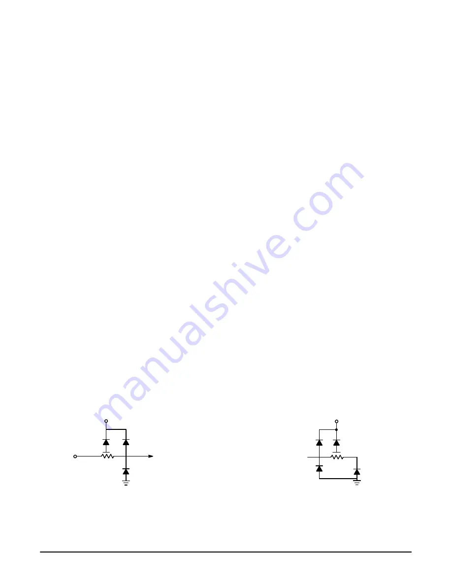
protection networks shown in Figures 1A and 1B are used on
each input to the CMOS device.
Static damaged devices behave in various ways, depend-
ing on the severity of the damage. The most severely dam-
aged inputs are the easiest to detect because the input has
been completely destroyed and is either shorted to VDD,
shorted to VSS, or open–circuited. The effect is that the de-
vice no longer responds to signals present at the damaged
input. Less severe cases are more difficult to detect because
they show up as intermittent failures or as degraded perfor-
mance. Another effect of static damage is that the inputs
generally have increased leakage currents.
Although the input protection network does provide a great
deal of protection, CMOS devices are not immune to large
static voltage discharges that can be generated during han-
dling. For example, static voltages generated by a person
walking across a waxed floor have been measured in the
4 –15 kV range (depending on humidity, surface conditions,
etc.). Therefore, the following precautions should be
observed:
1. Do not exceed the Maximum Ratings specified by the
data sheet.
2. All unused device inputs should be connected to VDD or
VSS.
3. All low–impedance equipment (pulse generators, etc.)
should be connected to CMOS inputs only after the de-
vice is powered up. Similarly, this type of equipment
should be disconnected before power is turned off.
4. Circuit boards containing CMOS devices are merely
extensions of the devices, and the same handling
precautions apply. Contacting edge connectors wired
directly to device inputs can cause damage. Plastic
wrapping should be avoided. When external connec-
tions to a PC board are connected to an input of a CMOS
device, a resistor should be used in series with the input.
This resistor helps limit accidental damage if the PC
board is removed and brought into contact with static
generating materials. The limiting factor for the series
resistor is the added delay. This is caused by the time
constant formed by the series resistor and input
capacitance. Note that the maximum input rise and fall
times should not be exceeded. In Figure 2, two possible
networks are shown using a series resistor to reduce
ESD (Electrostatic Discharge) damage. For conve-
nience, an equation for added propagation delay and
rise time effects due to series resistance size is given.
5. All CMOS devices should be stored or transported in
materials that are antistatic. CMOS devices must not be
inserted into conventional plastic “snow”, styrofoam, or
plastic trays, but should be left in their original container
until ready for use.
6. All CMOS devices should be placed on a grounded
bench surface and operators should ground them-
selves prior to handling devices, since a worker can be
statically charged with respect to the bench surface.
Wrist straps in contact with skin are strongly recom-
mended. See Figure 3 for an example of a typical work
station.
7. Nylon or other static generating materials should not
come in contact with CMOS devices.
8. If automatic handlers are being used, high levels of
static electricity may be generated by the movement of
the device, the belts, or the boards. Reduce static build–
up by using ionized air blowers or room humidifiers. All
parts of machines which come into contact with the top,
bottom, or sides of IC packages must be grounded to
metal or other conductive material.
9. Cold chambers using CO2 for cooling should be
equipped with baffles, and the CMOS devices must be
contained on or in conductive material.
10. When lead–straightening or hand–soldering is neces-
sary, provide ground straps for the apparatus used and
be sure that soldering ties are grounded.
INPUT PROTECTION NETWORK
Figure 1a. Input Protection Network
Double Diode
Figure 1b. Input Protection Network
Triple Diode
VDD
VDD
CMOS
INPUT
TO CIRCUIT
< 1500
Ω
VSS
CMOS
INPUT
300
Ω
VSS
Summary of Contents for CMOS Logic
Page 1: ......
Page 5: ...iv MOTOROLA CMOS LOGIC DATA ...
Page 6: ...Master Index 1 ...
Page 12: ...Product Selection Guide 2 ...
Page 17: ...The Better Program 3 ...
Page 20: ...B and UB Series Family Data 4 ...
Page 25: ...CMOS Handling and Design Guidelines 5 ...
Page 32: ...CMOS Handling and Design Guidelines 5 ...
Page 39: ...Data Sheets 6 ...
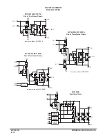
Page 234: ...MOTOROLA CMOS LOGIC DATA MC14174B 6 196 FUNCTIONAL BLOCK DIAGRAM TIMING DIAGRAM ...
Page 238: ...MOTOROLA CMOS LOGIC DATA MC14175B 6 200 FUNCTIONAL BLOCK DIAGRAM TIMING DIAGRAM ...
Page 555: ...CMOS Reliability 7 ...
Page 561: ...Equivalent Gate Count 8 ...
Page 563: ...Packaging Information Including Surface Mounts 9 ...
Page 571: ......

