MOTOROLA CMOS LOGIC DATA
6–309
MC14522B MC14526B
ÎÎÎÎÎÎÎÎÎÎÎÎÎÎÎÎÎÎÎÎÎÎÎÎÎÎÎÎÎÎÎÎÎÎ
ÎÎÎÎÎÎÎÎÎÎÎÎÎÎÎÎÎÎÎÎÎÎÎÎÎÎÎÎÎÎÎÎÎÎ
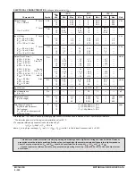
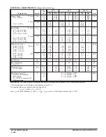
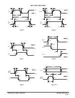
SWITCHING CHARACTERISTICS*
(CL = 50 pF, TA = 25
_
C)
Characteristic
Symbol
VDD
Min
Typ #
Max
Unit
Output Rise and Fall Time
tTLH, tTHL = (1.5 ns/pF) CL + 25 ns
tTLH, tTHL = (0.75 ns/pF) CL + 12.5 ns
tTLH, tTHL = (0.55 ns/pF) CL + 9.5 ns
tTLH,
tTHL
(Figures 4, 5)
5.0
10
15
—
—
—
100
50
40
200
100
80
ns
Propagation Delay Time (Inhibit Used as Negative
Edge Clock)
Clock or Inhibit to Q
tPLH, tPHL = (1.7 ns/pF) CL + 465 ns
tPLH, tPHL = (0.66 ns/pF) CL + 197 ns
tPLH, tPHL = (0.5 ns/pF) CL + 135 ns
tPLH,
tPHL
(Figures 4, 5, 6)
5.0
10
15
—
—
—
550
225
160
1100
450
320
ns
Clock or Inhibit to “0”
tPLH, tPHL = (1.7 ns/pF) CL + 155 ns
tPLH, tPHL = (0.66 ns/pF) CL + 87 ns
tPLH, tPHL = (0.5 ns/pF) CL + 65 ns
5.0
10
15
—
—
—
240
130
100
480
260
200
Propagation Delay Time
Pn to Q
tPLH,
tPHL
(Figures 4, 7)
5.0
10
15
—
—
—
260
120
100
520
240
200
ns
Propagation Delay Time
Reset to Q
tPHL
(Figure 8)
5.0
10
15
—
—
—
250
110
80
500
220
160
ns
Propagation Delay Time
Preset Enable to “0”
tPHL,
tPLH
(Figures 4, 9)
5.0
10
15
—
—
—
220
100
80
440
200
160
ns
Clock or Inhibit Pulse Width
tw
(Figures 5, 6)
5.0
10
15
250
100
80
125
50
40
—
—
—
ns
Clock Pulse Frequency (with PE = low)
fmax
(Figures 4, 5, 6)
5.0
10
15
—
—
—
2.0
5.0
6.6
1.5
3.0
4.0
MHz
Clock or Inhibit Rise and Fall Time
tr,
tf
(Figures 5, 6)
5.0
10
15
—
—
—
—
—
—
15
5
4
µ
s
Setup Time
Pn to Preset Enable
tsu
(Figure 10)
5.0
10
15
90
50
40
40
15
10
—
—
—
ns
Hold Time
Preset Enable to Pn
th
(Figure 10)
5.0
10
15
30
30
30
– 15
– 5
0
—
—
—
ns
Preset Enable Pulse Width
tw
(Figure 10)
5.0
10
15
250
100
80
125
50
40
—
—
—
ns
Reset Pulse Width
tw
(Figure 8)
5.0
10
15
350
250
200
175
125
100
—
—
—
ns
Reset Removal Time
trem
(Figure 8)
5.0
10
15
10
20
30
– 110
– 30
– 20
—
—
—
ns
* The formulas given are for the typical characteristics only at 25
_
C.
#Data labelled “Typ” is not to be used for design purposes but is intended as an indication of the IC’s potential performance.
Summary of Contents for CMOS Logic
Page 1: ......
Page 5: ...iv MOTOROLA CMOS LOGIC DATA ...
Page 6: ...Master Index 1 ...
Page 12: ...Product Selection Guide 2 ...
Page 17: ...The Better Program 3 ...
Page 20: ...B and UB Series Family Data 4 ...
Page 25: ...CMOS Handling and Design Guidelines 5 ...
Page 32: ...CMOS Handling and Design Guidelines 5 ...
Page 39: ...Data Sheets 6 ...
Page 234: ...MOTOROLA CMOS LOGIC DATA MC14174B 6 196 FUNCTIONAL BLOCK DIAGRAM TIMING DIAGRAM ...
Page 238: ...MOTOROLA CMOS LOGIC DATA MC14175B 6 200 FUNCTIONAL BLOCK DIAGRAM TIMING DIAGRAM ...
Page 555: ...CMOS Reliability 7 ...
Page 561: ...Equivalent Gate Count 8 ...
Page 563: ...Packaging Information Including Surface Mounts 9 ...
Page 571: ......


