CHAPTER 5
5–4
MOTOROLA CMOS LOGIC DATA
Figure 2. Typical Manufacturing Work Station
RESISTOR =
1 MEGAOHM
1
2
3
4
5
NOTES: 1. 1/16 inch conductive sheet stock covering bench
top work area.
2. Ground strap.
3. Wrist strap in contact with skin.
4. Static neutralizer. (Ionized air blower directed at
work.) Primarily for use in areas where direct
grounding is impractical.
5. Room humidifier. Primarily for use in areas where
the relative humidity is less than 45%. Caution:
building heating and cooling systems usually dry
the air causing the relative humidity inside of
buildings to be less than outside humidity.
POWER SUPPLIES
CMOS devices have low power requirements and the abil-
ity to operate over a wide range of supply voltages. These
two characteristics allow CMOS designs to be implemented
using inexpensive, conventional power supplies, instead of
switching power supplies and power supplies with cooling
fans. In addition, batteries may be used as either a primary
power source or for emergency backup.
The
absolute maximum power supply voltage for 14000
Series Metal–gate CMOS is 18.0 Vdc. Figure 4 offers some
insight as to how this specification was derived. In the figure,
VS is the maximum power supply voltage and IS is the sus-
taining current of the latch–up mode. The value of VS was
chosen so that the secondary breakdown effect may be
avoided.
In an ideal system design, a power supply should be
designed to deliver only enough current to insure proper
operation of all devices. The obvious benefit of this type
design is cost savings; an added benefit is protection against
the possibility of latch–up related failures. This system
protection can be provided by the power supply filter and/or
voltage regulator.
CMOS devices can be used with battery or battery backup
systems. A few precautions should be taken when designing
battery–operated systems:
1. The recommended power supply voltage should be ob-
served. For battery backup systems such as the one in
Figure 5, the battery voltage must be at least 3.7 Volts
(3 Volts from the minimum power supply voltage and
0.7 Volts to account for the voltage drop across the se-
ries diode).
2. Inputs that might go above the battery backup voltage
should either use a series resistor to limit the input cur-
rent to less than 10 mA or use the MC14049UB or
MC14050B high–to–low voltage translators.
3. Outputs that are subject to voltage levels above VDD or
below VSS should be protected with a series resistor to
limit the current to less than 10 mA or with clamping
diodes.
Figure 3. Secondary Breakdown Characteristics
IDD
IS
VS
VDD
LATCH
UP MODE
SECONDARY
BREAKDOWN
LOW CURRENT
JUNCTION
AVALANCHE
VS = DATA SHEET MAXIMUM SUPPLY RATING
Summary of Contents for CMOS Logic
Page 1: ......
Page 5: ...iv MOTOROLA CMOS LOGIC DATA ...
Page 6: ...Master Index 1 ...
Page 12: ...Product Selection Guide 2 ...
Page 17: ...The Better Program 3 ...
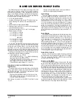
Page 20: ...B and UB Series Family Data 4 ...
Page 25: ...CMOS Handling and Design Guidelines 5 ...
Page 32: ...CMOS Handling and Design Guidelines 5 ...
Page 39: ...Data Sheets 6 ...
Page 234: ...MOTOROLA CMOS LOGIC DATA MC14174B 6 196 FUNCTIONAL BLOCK DIAGRAM TIMING DIAGRAM ...
Page 238: ...MOTOROLA CMOS LOGIC DATA MC14175B 6 200 FUNCTIONAL BLOCK DIAGRAM TIMING DIAGRAM ...
Page 555: ...CMOS Reliability 7 ...
Page 561: ...Equivalent Gate Count 8 ...
Page 563: ...Packaging Information Including Surface Mounts 9 ...
Page 571: ......

