MOTOROLA CMOS LOGIC DATA
MC14529B
6–330
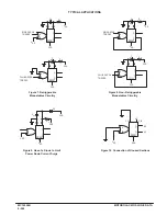
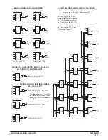
Figure 1. Output Voltage
Test Circuit
Figure 2. Noise Immunity
Test Circuit
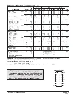
Pins 2, 3, 4, 12, 13 and 14 are left open.
VIL: VC is raised from VSS until VC = VIL.
VIL:
at VC = VIL: IS =
±
10
µ
A with Vin = VSS, Vout = VDD
VIL:
Vin = VDD, Vout = VSS.
VIH: When VC = VIH to VDD, the switch is ON and the RON
VIH:
specifications are met.
V
VDD
Vin
VSS = 0.0 V
VSS
OUT
VN
1 k
VDD
VSS
IS
Z
W
STX
STY
A
B
X3
Y3
Figure 3. Quiescent Power Dissipation
Test Circuit
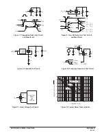
Figure 4. RON Characteristics
Test Circuit
PULSE
GENERATOR
VDD
OUT
10 k
VSS
Vin
ID
VDD
fc
A0, A1
PD = VDD x ID
VDD
OUT
VSS
Vin
RL
STX = STY = VDD
TYPICAL RON versus INPUT VOLTAGE
Figure 5.
Figure 6.
Vin, INPUT VOLTAGE (Vdc)
Vin, INPUT VOLTAGE (Vdc)
–10
–5
0
5
10
0
5
10
15
20
25
VDD = 15 V
VSS = 0 V
VDD = 10 V
VSS = 0 V
VDD = 5 V
VSS = –5 V
VDD = 7.5 V
VSS = –7.5 V
R “ON” RESIST
ANCE
(OHMS)
ON
R “ON” RESIST
ANCE
(OHMS)
ON
250
200
150
100
50
0
250
200
150
100
50
0
Summary of Contents for CMOS Logic
Page 1: ......
Page 5: ...iv MOTOROLA CMOS LOGIC DATA ...
Page 6: ...Master Index 1 ...
Page 12: ...Product Selection Guide 2 ...
Page 17: ...The Better Program 3 ...
Page 20: ...B and UB Series Family Data 4 ...
Page 25: ...CMOS Handling and Design Guidelines 5 ...
Page 32: ...CMOS Handling and Design Guidelines 5 ...
Page 39: ...Data Sheets 6 ...
Page 234: ...MOTOROLA CMOS LOGIC DATA MC14174B 6 196 FUNCTIONAL BLOCK DIAGRAM TIMING DIAGRAM ...
Page 238: ...MOTOROLA CMOS LOGIC DATA MC14175B 6 200 FUNCTIONAL BLOCK DIAGRAM TIMING DIAGRAM ...
Page 555: ...CMOS Reliability 7 ...
Page 561: ...Equivalent Gate Count 8 ...
Page 563: ...Packaging Information Including Surface Mounts 9 ...
Page 571: ......


