MOTOROLA CMOS LOGIC DATA
6–357
MC14536B
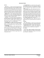
PIN DESCRIPTIONS
INPUTS
SET (Pin 1) — A high on Set asynchronously forces
Decode Out to a high level. This is accomplished by setting
an output conditioning latch to a high level while at the same
time resetting the 24 flip–flop stages. After Set goes low
(inactive), the occurrence of the first negative clock transition
on IN1 causes Decode Out to go low. The counter’s flip–flop
stages begin counting on the second negative clock transi-
tion of IN1. When Set is high, the on–chip RC oscillator is
disabled. This allows for very low–power standby operation.
RESET (Pin 2) — A high on Reset asynchronously forces
Decode Out to a low level; all 24 flip–flop stages are also
reset to a low level. Like the Set input, Reset disables the
on–chip RC oscillator for standby operation.
IN1 (Pin 3) — The device’s internal counters advance on
the negative–going edge of this input. IN1 may be used as an
external clock input or used in conjunction with OUT1 and
OUT2 to form an RC oscillator. When an external clock is
used, both OUT1 and OUT2 may be left unconnected or
used to drive 1 LSTTL or several CMOS loads.
8–BYPASS (Pin 6) — A high on this input causes the first
8 flip–flop stages to be bypassed. This device essentially be-
comes a 16–stage counter with all 16 stages selectable.
Selection is accomplished by the A, B, C, and D inputs. (See
the truth tables.)
CLOCK INHIBIT (Pin 7) — A high on this input discon-
nects the first counter stage from the clocking source. This
holds the present count and inhibits further counting. How-
ever, the clocking source may continue to run. Therefore,
when Clock Inhibit is brought low, no oscillator start–up time
is required. When Clock Inhibit is low, the counter will start
counting on the occurrence of the first negative edge of the
clocking source at IN1.
OSC INHIBIT (Pin 14) — A high level on this pin stops the
RC oscillator which allows for very low–power standby op-
eration. May also be used, in conjunction with an external
clock, with essentially the same results as the Clock Inhibit
input.
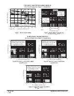
MONO–IN (Pin 15) — Used as the timing pin for the on–
chip monostable multivibrator. If the Mono–In input is con-
nected to VSS, the monostable circuit is disabled, and
Decode Out is directly connected to the selected Q output.
The monostable circuit is enabled if a resistor is connected
between Mono–In and VDD. This resistor and the device’s in-
ternal capacitance will determine the minimum output pulse
widths. With the addition of an external capacitor to VSS, the
pulse width range may be extended. For reliable operation
the resistor value should be limited to the range of 5 k
Ω
to
100 k
Ω
and the capacitor value should be limited to a maxi-
mum of 1000 pf. (See figures 3, 4, 5, and 10).
A, B, C, D (Pins 9, 10, 11, 12) — These inputs select the
flip–flop stage to be connected to Decode Out. (See the truth
tables.)
OUTPUTS
OUT1, OUT2 (Pin 4, 5) — Outputs used in conjunction with
IN1 to form an RC oscillator. These outputs are buffered and
may be used for 20 frequency division of an external clock.
DECODE OUT (Pin 13) — Output function depends on
configuration. When the monostable circuit is disabled, this
output is a 50% duty cycle square wave during free run.
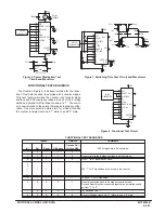
TEST MODE
The test mode configuration divides the 24 flip–flop stages
into three 8–stage sections to facilitate a fast test sequence.
The test mode is enabled when 8–Bypass, Set and Reset
are at a high level. (See Figure 8.)
Summary of Contents for CMOS Logic
Page 1: ......
Page 5: ...iv MOTOROLA CMOS LOGIC DATA ...
Page 6: ...Master Index 1 ...
Page 12: ...Product Selection Guide 2 ...
Page 17: ...The Better Program 3 ...
Page 20: ...B and UB Series Family Data 4 ...
Page 25: ...CMOS Handling and Design Guidelines 5 ...
Page 32: ...CMOS Handling and Design Guidelines 5 ...
Page 39: ...Data Sheets 6 ...
Page 234: ...MOTOROLA CMOS LOGIC DATA MC14174B 6 196 FUNCTIONAL BLOCK DIAGRAM TIMING DIAGRAM ...
Page 238: ...MOTOROLA CMOS LOGIC DATA MC14175B 6 200 FUNCTIONAL BLOCK DIAGRAM TIMING DIAGRAM ...
Page 555: ...CMOS Reliability 7 ...
Page 561: ...Equivalent Gate Count 8 ...
Page 563: ...Packaging Information Including Surface Mounts 9 ...
Page 571: ......


