MOTOROLA CMOS LOGIC DATA
6–377
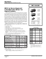
MC14541B
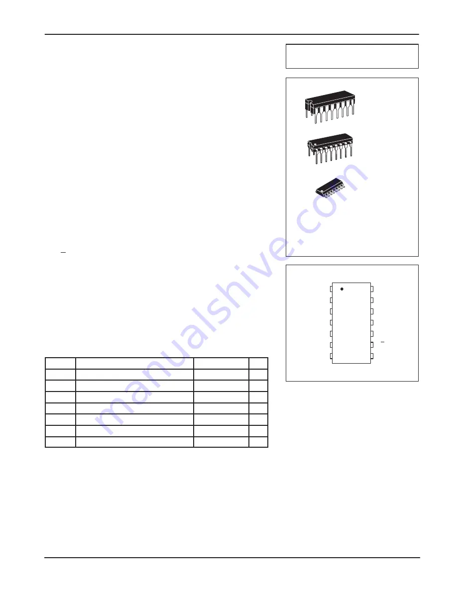
Programmable Timer
The MC14541B programmable timer consists of a 16–stage binary
counter, an integrated oscillator for use with an external capacitor and two
resistors, an automatic power–on reset circuit, and output control logic.
Timing is initialized by turning on power, whereupon the power–on reset is
enabled and initializes the counter, within the specified VDD range. With the
power already on, an external reset pulse can be applied. Upon release of
the initial reset command, the oscillator will oscillate with a frequency
determined by the external RC network. The 16–stage counter divides the
oscillator frequency (fosc) with the nth stage frequency being fosc/2n.
•
Available Outputs 28, 210, 213 or 216
•
Increments on Positive Edge Clock Transitions
•
Built–in Low Power RC Oscillator (
±
2% accuracy over temperature
range and
±
20% supply and
±
3% over processing at < 10 kHz)
•
Oscillator May Be Bypassed if External Clock Is Available (Apply
external clock to Pin 3)
•
External Master Reset Totally Independent of Automatic Reset
Operation
•
Operates as 2n Frequency Divider or Single Transition Timer
•
Q/Q Select Provides Output Logic Level Flexibility
•
Reset (auto or master) Disables Oscillator During Resetting to Provide
No Active Power Dissipation
•
Clock Conditioning Circuit Permits Operation with Very Slow Clock Rise
and Fall Times
•
Automatic Reset Initializes All Counters On Power Up
•
Supply Voltage Range = 3.0 Vdc to 18 Vdc with Auto Reset
Disabled (Pin 5 = VDD)
= 8.5 Vdc to 18 Vdc with Auto Reset
Enabled (Pin 5 = VSS)
ÎÎÎÎÎÎÎÎÎÎÎÎÎÎÎÎÎÎÎÎÎ
ÎÎÎÎÎÎÎÎÎÎÎÎÎÎÎÎÎÎÎÎÎ
MAXIMUM RATINGS*
(Voltages Referenced to VSS)
ÎÎÎÎ
ÎÎÎÎ
Symbol
ÎÎÎÎÎÎÎÎÎÎÎ
ÎÎÎÎÎÎÎÎÎÎÎ
Parameter
ÎÎÎÎÎÎ
ÎÎÎÎÎÎ
Value
ÎÎÎ
ÎÎÎ
Unit
ÎÎÎÎ
ÎÎÎÎ
VDD
ÎÎÎÎÎÎÎÎÎÎÎ
ÎÎÎÎÎÎÎÎÎÎÎ
DC Supply Voltage
ÎÎÎÎÎÎ
ÎÎÎÎÎÎ
– 0.5 to + 18.0
ÎÎÎ
ÎÎÎ
V
ÎÎÎÎ
ÎÎÎÎ
Vin, Vout
ÎÎÎÎÎÎÎÎÎÎÎ
ÎÎÎÎÎÎÎÎÎÎÎ
Input or Output Voltage (DC or Transient)
ÎÎÎÎÎÎ
ÎÎÎÎÎÎ
– 0.5 to VDD + 0.5
ÎÎÎ
ÎÎÎ
V
ÎÎÎÎ
ÎÎÎÎ
Iin
ÎÎÎÎÎÎÎÎÎÎÎ
ÎÎÎÎÎÎÎÎÎÎÎ
Input Current (DC or Transient), per Pin
ÎÎÎÎÎÎ
ÎÎÎÎÎÎ
±
10
ÎÎÎ
ÎÎÎ
mA
ÎÎÎÎ
ÎÎÎÎ
Iout
ÎÎÎÎÎÎÎÎÎÎÎ
ÎÎÎÎÎÎÎÎÎÎÎ
Output Current (DC or Transient), per Pin
ÎÎÎÎÎÎ
ÎÎÎÎÎÎ
±
45
ÎÎÎ
ÎÎÎ
mA
ÎÎÎÎ
ÎÎÎÎ
PD
ÎÎÎÎÎÎÎÎÎÎÎ
ÎÎÎÎÎÎÎÎÎÎÎ
Power Dissipation, per Package†
ÎÎÎÎÎÎ
ÎÎÎÎÎÎ
500
ÎÎÎ
ÎÎÎ
mW
ÎÎÎÎ
ÎÎÎÎ
Tstg
ÎÎÎÎÎÎÎÎÎÎÎ
ÎÎÎÎÎÎÎÎÎÎÎ
Storage Temperature
ÎÎÎÎÎÎ
ÎÎÎÎÎÎ
– 65 to + 150
ÎÎÎ
ÎÎÎ
_
C
ÎÎÎÎ
ÎÎÎÎ
TL
ÎÎÎÎÎÎÎÎÎÎÎ
ÎÎÎÎÎÎÎÎÎÎÎ
Lead Temperature (8–Second Soldering)
ÎÎÎÎÎÎ
ÎÎÎÎÎÎ
260
ÎÎÎ
ÎÎÎ
_
C
* Maximum Ratings are those values beyond which damage to the device may occur.
†Temperature Derating:
Plastic “P and D/DW” Packages: – 7.0 mW/
_
C From 65
_
C To 125
_
C
Ceramic “L” Packages: – 12 mW/
_
C From 100
_
C To 125
_
C
MOTOROLA
SEMICONDUCTOR TECHNICAL DATA
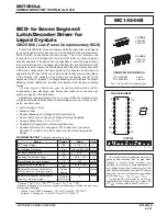
MC14541B
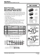
L SUFFIX
CERAMIC
CASE 620
ORDERING INFORMATION
MC14XXXBCP
Plastic
MC14XXXBCL
Ceramic
MC14XXXBD
SOIC
TA = – 55
°
to 125
°
C for all packages.
P SUFFIX
PLASTIC
CASE 648
D SUFFIX
SOIC
CASE 751B
PIN ASSIGNMENT
NC = NO CONNECTION
11
12
13
14
8
9
10
5
4
3
2
1
7
6
MODE
NC
A
B
VDD
Q
Q/Q SEL
NC
RS
Ctc
Rtc
VSS
MR
AR
Summary of Contents for CMOS Logic
Page 1: ......
Page 5: ...iv MOTOROLA CMOS LOGIC DATA ...
Page 6: ...Master Index 1 ...
Page 12: ...Product Selection Guide 2 ...
Page 17: ...The Better Program 3 ...
Page 20: ...B and UB Series Family Data 4 ...
Page 25: ...CMOS Handling and Design Guidelines 5 ...
Page 32: ...CMOS Handling and Design Guidelines 5 ...
Page 39: ...Data Sheets 6 ...
Page 234: ...MOTOROLA CMOS LOGIC DATA MC14174B 6 196 FUNCTIONAL BLOCK DIAGRAM TIMING DIAGRAM ...
Page 238: ...MOTOROLA CMOS LOGIC DATA MC14175B 6 200 FUNCTIONAL BLOCK DIAGRAM TIMING DIAGRAM ...
Page 555: ...CMOS Reliability 7 ...
Page 561: ...Equivalent Gate Count 8 ...
Page 563: ...Packaging Information Including Surface Mounts 9 ...
Page 571: ......


