MOTOROLA CMOS LOGIC DATA
6–427
MC14557B
ÎÎÎÎÎÎÎÎÎÎÎÎÎÎÎÎÎÎÎÎÎÎÎÎÎÎÎÎÎÎÎÎÎÎ
ÎÎÎÎÎÎÎÎÎÎÎÎÎÎÎÎÎÎÎÎÎÎÎÎÎÎÎÎÎÎÎÎÎÎ
SWITCHING CHARACTERISTICS*
(CL = 50 pF, TA = 25
_
C)
Characteristic
Symbol
VDD
Min
Typ #
Max
Unit
Rise and Fall Time, Q or Q Output
tTLH, tTHL = (1.5 ns/pF) CL + 25 ns
tTLH, tTHL = (0.75 ns/pF) CL + 12.5 ns
tTLH, tTHL = (0.55 ns/pF) CL + 9.5 ns
tTLH,
tTHL
5
10
15
—
—
—
100
50
40
200
100
80
ns
Propagation Delay, Clock or CE to Q or Q
tPLH, tPHL = (1.7 ns/pF) CL + 215 ns
tPLH, tPHL = (0.66 ns/pF) CL + 97 ns
tPLH, tPHL = (0.5 ns/pF) CL + 65 ns
tPLH,
tPHL
5
10
15
—
—
—
300
130
90
600
260
180
ns
Propagation Delay, Reset to Q or Q
tPLH, tPHL = (1.7 ns/pF) CL + 215 ns
tPLH, tPHL = (0.66 ns/pF) CL + 97 ns
tPLH, tPHL = (0.5 ns/pF) CL + 70 ns
tPLH,
tPHL
5
10
15
—
—
—
300
130
95
600
260
190
ns
Pulse Width, Clock
tWH(cl)
5
10
15
200
100
75
95
45
35
—
—
—
ns
Pulse Width, Reset
tWH(rst)
5
10
15
300
140
100
150
70
50
—
—
—
ns
Clock Frequency (50% Duty Cycle)
fcl
5
10
15
—
—
—
3.0
7.5
13.0
1.7
5.0
6.7
MHz
Setup Time, A or B to Clock or CE
Worst case condition: L1 = L2 = L4 = L8 =
L16 = L32 = VSS (Register Length = 1)
tsu
5
10
15
700
290
145
350
130
85
—
—
—
ns
Best case condition: L32 = VDD, L1 through L16 =
Don’t Care (Any register length from 33 to 64)
5
10
15
400
165
60
45
5
0
—
—
—
Hold Time, Clock or CE to A or B
Best case condition: L1 = L2 = L4 = L8 = L16 =
L32 = VSS (Register Length = 1)
th
5
10
15
200
100
10
– 150
– 60
– 50
—
—
—
ns
Worst case condition: L32 = VDD, L1 through L16 =
Don’t Care (Any register length from 33 to 64)
5
10
15
400
185
85
50
25
22
—
—
—
Rise and Fall Time, Clock
tr,
tf
5
10
15
No Limit
—
Rise and Fall Time, Reset or CE
tr,
tf
5
10
15
—
—
—
—
—
—
15
5
4
µ
s
Removal Time, Reset to Clock or CE
trem
5
10
15
160
80
70
80
40
35
—
—
—
ns
* The formulas given are for the typical characteristics only at 25
_
C.
# Data labelled “Typ” is not to be used for design purposes but is intended as an indication of the IC’s potential performance.
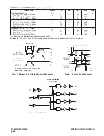
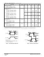
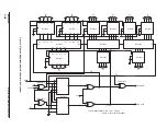
TIMING DIAGRAM
1–bit length:
CE = 0
A/B = 1
L1 = L2 = L4 = L8 = L16 = L32 = 0
PWR
50%
tWH(cl)
th
50%
tsu
trem
50%
tTLH
tTHL
tPHL
tPHL
tPLH
90%
50%
10%
A INPUT
CLOCK
RESET
Q
VDD
VSS
VDD
VSS
VDD
VSS
VOH
VOL
1/fcl
Summary of Contents for CMOS Logic
Page 1: ......
Page 5: ...iv MOTOROLA CMOS LOGIC DATA ...
Page 6: ...Master Index 1 ...
Page 12: ...Product Selection Guide 2 ...
Page 17: ...The Better Program 3 ...
Page 20: ...B and UB Series Family Data 4 ...
Page 25: ...CMOS Handling and Design Guidelines 5 ...
Page 32: ...CMOS Handling and Design Guidelines 5 ...
Page 39: ...Data Sheets 6 ...
Page 234: ...MOTOROLA CMOS LOGIC DATA MC14174B 6 196 FUNCTIONAL BLOCK DIAGRAM TIMING DIAGRAM ...
Page 238: ...MOTOROLA CMOS LOGIC DATA MC14175B 6 200 FUNCTIONAL BLOCK DIAGRAM TIMING DIAGRAM ...
Page 555: ...CMOS Reliability 7 ...
Page 561: ...Equivalent Gate Count 8 ...
Page 563: ...Packaging Information Including Surface Mounts 9 ...
Page 571: ......


