MOTOROLA CMOS LOGIC DATA
6–51
MC14016B
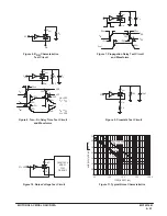
Figure 6. RON Characteristics
Test Circuit
Figure 7. Propagation Delay Test Circuit
and Waveforms
VC
Vin
Vout
RL
Vout
Vin
RL
CL
20 ns
20 ns
VDD
VSS
Vin
Vout
tPLH
tPHL
50%
10%
50%
90%
Figure 8. Turn–On Delay Time Test Circuit
and Waveforms
Figure 9. Crosstalk Test Circuit
VC
Vout
Vin
RL
CL
VX
20 ns
VC
Vout
Vout
10%
90%
10%
90%
90%
50%
10%
tPZH
tPHZ
VDD
VSS
tPLZ
tPZL
Vin = VDD
Vx = VSS
Vin = VSS
Vx = VDD
VC
Vout
Vin
1 k
10 k
15 pF
Figure 10. Noise Voltage Test Circuit
Figure 11. Typical Noise Characteristics
VC = VDD
OUT
IN
QUAN–TECH
MODEL
2283
OR EQUIV
100 k
10 k
1.0 k
100
10
35
30
25
20
0
10 Vdc
5.0 Vdc
f, FREQUENCY (Hz)
NOISE VOL
TAGE (nV/
CYCLE)
15
10
5.0
VDD = 15 Vdc
Summary of Contents for CMOS Logic
Page 1: ......
Page 5: ...iv MOTOROLA CMOS LOGIC DATA ...
Page 6: ...Master Index 1 ...
Page 12: ...Product Selection Guide 2 ...
Page 17: ...The Better Program 3 ...
Page 20: ...B and UB Series Family Data 4 ...
Page 25: ...CMOS Handling and Design Guidelines 5 ...
Page 32: ...CMOS Handling and Design Guidelines 5 ...
Page 39: ...Data Sheets 6 ...
Page 234: ...MOTOROLA CMOS LOGIC DATA MC14174B 6 196 FUNCTIONAL BLOCK DIAGRAM TIMING DIAGRAM ...
Page 238: ...MOTOROLA CMOS LOGIC DATA MC14175B 6 200 FUNCTIONAL BLOCK DIAGRAM TIMING DIAGRAM ...
Page 555: ...CMOS Reliability 7 ...
Page 561: ...Equivalent Gate Count 8 ...
Page 563: ...Packaging Information Including Surface Mounts 9 ...
Page 571: ......


