4-1
4
4
Functional Description
This chapter provides a functional description of all major components and
devices on the CPN5365.
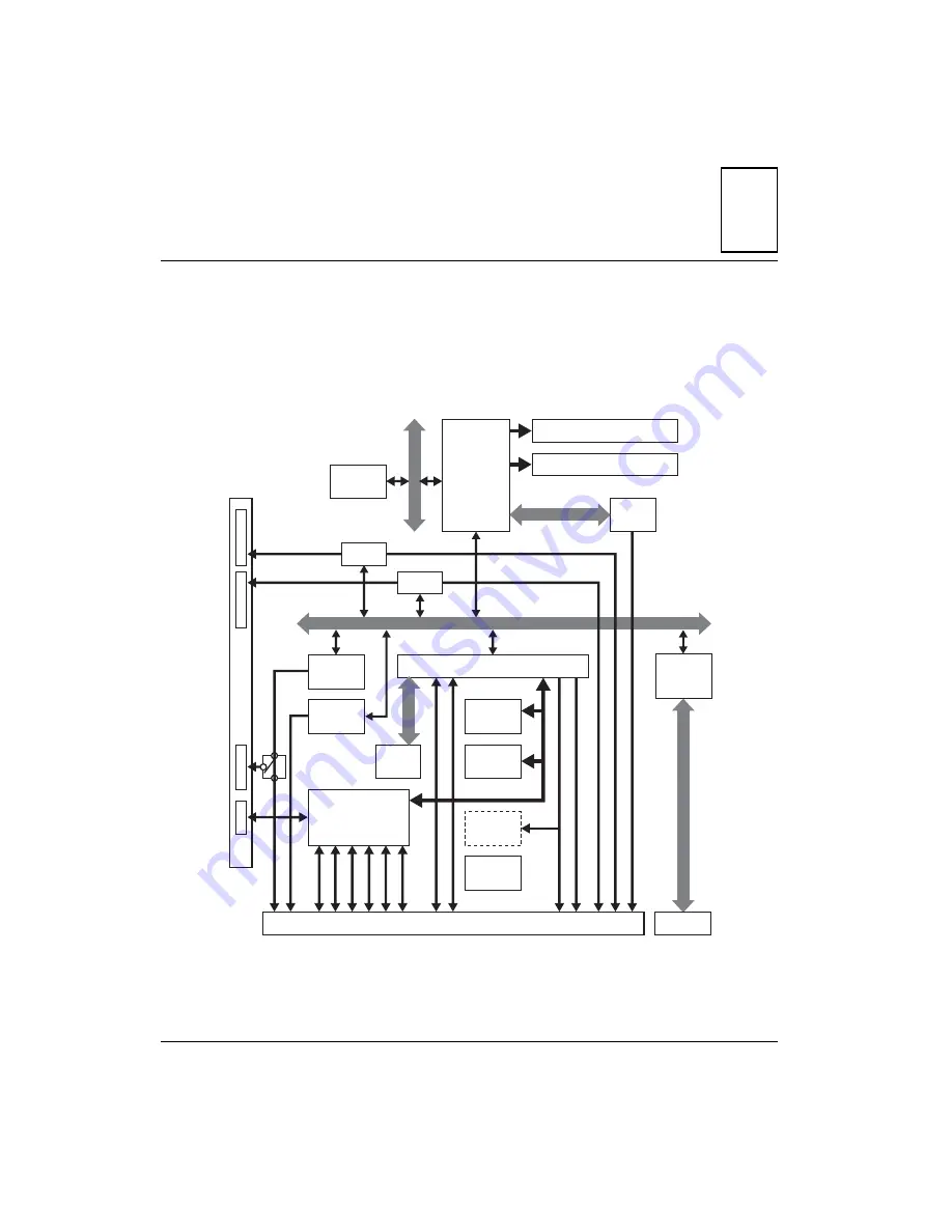
The following block diagram illustrates the major components and their
circuitry on the CPN5365 Single Board Computer.
Figure 4-1. Block Diagram of CPN5365
4290 0804
33 MHZ, 64 bit PCI Local Bus
User VO J3, J5 & J4
ISA Bridge (South Bridge)
Intel PIIX4E
Ethernet 2
Intel 82559
Ethernet 1
Intel 82559
Ultra I/O
Ethernet
33 MHZ, 64 bit CPCI Bus
CPCI J1/J2
COM
PMC I/O
PMC I/O
Ethernet 1 J5
Ethernet 2 J5
COM 1 J3
COM 2 J3
KBD J5
Mouse J5
Printer J4
Floppy J4
USB 0 J3
USB 1 J3
ISA
System
Monitor
Flash
BIOS
Flash
BIOS
FPGA
On-Card
Hard Drive
(Optional)
System
Monitor
PCI to PCI
Bridge
Intel 21154
SM Bus
Primary IDE J4
Secondary IDE
PMC 2 I/O J5
PMC 1 I/O J3
Video J4
AGP
Video
PMC 2
PMC 2
PMC 2
Processor
PCI Bridge
and
Memory
Controller
(North Bridge
Intel 440GX)
100 MHz Processor
AGP Bus
Soldered-on memory: to 512MB
Memory mezzaine: to 512MB


