2-2
Recommended Operating Conditions
2.3 Recommended Operating Conditions
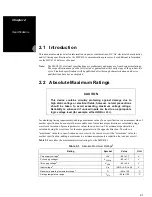
Table 2-2 lists recommended operating conditions. Proper device operation outside of these conditions is
not guaranteed.
2.4 Thermal Characteristics
Table 2-3 describes thermal characteristics of the MSC8101.
Notes:
1.
Functional operating conditions are given in Table 2-2.
2.
Absolute maximum ratings are stress ratings only, and functional operation at the maximum is not
guaranteed. Stress beyond the listed limits may affect device reliability or cause permanent damage.
3.
The input voltage must not exceed the I/O supply V
DDH
by more than 2.5 V at any time, including
during power-on reset. In turn, V
DDH
can exceed V
DD
/V
CCSYN
by more than 3.3 V during power-on
reset, but for no more than 100 ms. V
DDH
should not exceed V
DD
/V
CCSYN
by more than 2.1 V during
normal operation. V
DD
/V
CCSYN
must not exceed V
DDH
by more than 0.4 V at any time, including
during power-on reset. See Section 4.2,
Electrical Design Considerations
, on page 4-2 for more
information.
4.
Section 4.1,
Thermal Design Considerations
, on page 4-1 includes a formula for computing the chip
junction temperature (T
J
).
Table 2-2. Recommended Operating Conditions
Rating
Symbol
Value
Unit
SC140 Core supply voltage
V
DD
1.5 to 1.7
V
PLL supply voltage
V
CCSYN
1.5 to 1.7
V
I/O supply voltage
V
DDH
3.135 to 3.465
V
Input voltage
V
IN
–0.2 to V
DDH
+ 0.2
V
Operating temperature range
T
J
–40 to 105
°C
Table 2-3. Thermal Characteristics
Characteristic
Symbol
FC-PBGA
17
×
17mm
Unit
Junction-to-ambient
1, 2
R
θ
JA
or
θ
JA
52
°C/W
Junction-to-ambient, four-layer board
1, 3
R
θ
JA
or
θ
JA
25
°C/W
Junction-to-board (bottom)
4
R
θ
JB
or
θ
JB
22
°C/W
Junction-to-case (top)
5
R
θ
JC
or
θ
JC
0.3
°C/W
Junction-to-package (top)
6
ψ
JT
0.3
°C/W
Notes:
1.
Junction temperature is a function of on-chip power dissipation, package thermal resistance, mounting
site (board) temperature, ambient temperature, air flow, power dissipation of other components on the
board, and board thermal resistance.
2.
Per SEMI G38-87 and EIA/JESD51-2 with the single layer (1s) board horizontal.
3.
Per JESD51-6 with the boards horizontal.
4.
Thermal resistance between the die and the printed circuit board per JESD 51-8.
5.
Indicates the average thermal resistance between the die and the case top surface as measured by the
cold plate method (MIL SPEC-883 Method 1012.1) with the cold plate temperature used for case
temperature.
6.
Thermal characterization parameter indicating the temperature difference between package top and
the junction temperature, per EIA/JESD51-2.
Table 2-1. Absolute Maximum Ratings
2
(Continued)
Rating
Symbol
Value
Unit


