


2-3
DC Electrical Characteristics
See Section 4.1, Thermal Design Considerations, on page 4-1 for details on these characteristics.
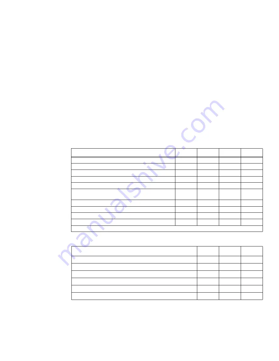
2.5 DC Electrical Characteristics
This section describes the DC electrical characteristics for the MSC8101. The measurements in Table 2-4
assume the following system conditions:
• T
J
= 0 – 100 °C
•
V
DD
= 1.6 V ± 5% V
DC
•
V
DDH
= 3.3 V ± 5% V
DC
•
GND
= 0 V
DC
Note:
The leakage current is measured for nominal
V
DDH
and
V
DD
or both
V
DDH
and
V
DD
must vary in
the same direction (for example, both
V
DDH
and
V
DD
vary by ± 5 percent).
Table 2-4. DC Electrical Characteristics
Characteristic
Symbol
Min
Max
Unit
Input high voltage, all inputs except CLKIN
V
IH
2.0
3.465
V
Input low voltage
V
IL
GND
0.8
V
CLKIN input high voltage
V
IHC
2.5
3.465
V
CLKIN input low voltage
1
V
ILC
GND
0.8
V
Input leakage current, V
IN
= V
DDH
I
IN
—
10
µA
Tri-state (high impedance off state) leakage current,
V
IN
= V
DDH
I
OZ
—
10
µA
Signal low input current, V
IL
= 0.4 V
I
L
—
–4.0
mA
Signal high input current, V
IH
= 2.0 V
I
H
—
4.0
mA
Output high voltage, I
OH
= –2 mA, except open drain pins
V
OH
2.4
—
V
Output low voltage, I
OL
= 3.2 mA
V
OL
—
0.4
V
Notes:
1.
The optimum CLKIN duty cycle is obtained when: V
ILC
= V
DDH
– V
IHC
.
Table 2-5. Typical Power Dissipation
Characteristic
Symbol
Typical
Unit
Core power dissipation at 300 MHz
P
CORE
350
mW
CPM power dissipation at 150 MHz
P
CPM
240
mW
SIU power dissipation at 100 MHz
P
SIU
80
mW
Core leakage power
P
LCO
3
mW
Input/Output Ports leakage power
P
LCP
6
mW
SIU leakage power
P
LSI
2
mW


