1-2
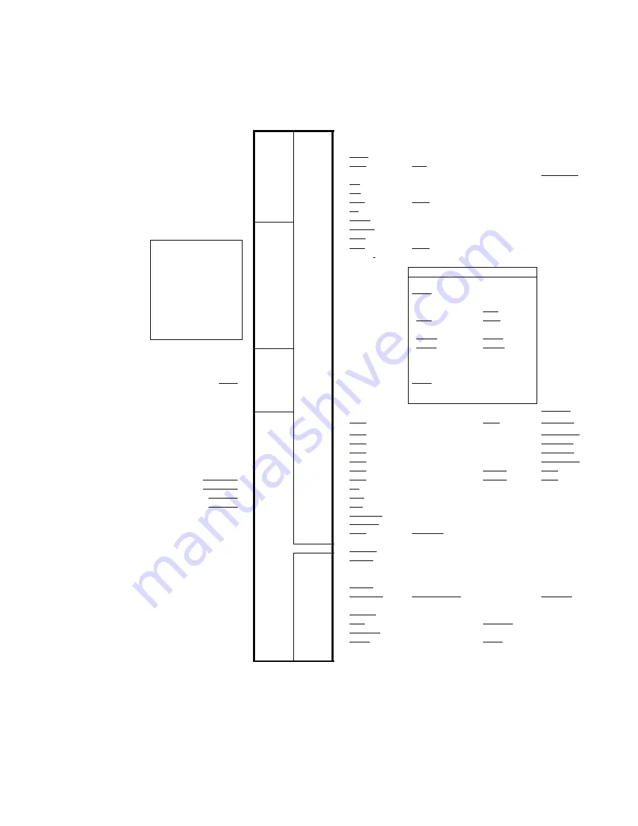
Signal Groupings
P
O
W
E
R
6
0
x
B
U
S
32
↔
A[0–31]
VDD
→
14
5
↔
TT[0–4]
VDDH
→
25
4
↔
TSIZ[0–3]
VCCSYN
→
1
1
↔
TBST
VCCSYN1
→
1
1
↔
IRQ1
GBL
3
→
Reserved
BADDR[29–31]
IRQ[2–3, 5]
GND
→
37
1
↔
BR
GNDSYN
→
1
1
↔
BG
GNDSYN1
→
1
1
↔
ABB
IRQ2
1
↔
TS
C
P
M
I
/
O
P
O
R
T
S
1
↔
AACK
1
←
ARTRY
For the signals
multiplexed on
Ports A–D,
see Figure 1-2
Port A
1
↔
DBG
PA[31–6]
↔
26
1
↔
DBB
IRQ3
32
↔
D[0–31]
Port B
HDI16 Signals
PB[31–18]
↔
14
16
↔
D[32–47]
HD[0–15]
4
↔
D[48–51]
HA[0–3]
Port C
1
↔
D52
HCS1
PC[31–22, 15–12, 7–4]
↔
18
Single DS
Double DS
1
↔
D53
HRW
HRD/HRD
Port D
1
↔
D54
HDS/HDS
HWR/HWR
PD[31–29, 19–16, 7]
↔
8
Single HR
Double HR
1
↔
D55
HREQ/HREQ
HTRQ/HTRQ
J
T
A
G
1
↔
D56
HACK/HACK
HRRQ/HRRQ
TMS
→
1
1
↔
D57
HDSP
TDI
→
1
1
↔
D58
HDDS
TCK
→
1
1
↔
D59
H8BIT
TRST
→
1
1
↔
D60
HCS2
TDO
←
1
4
↔
D[61–63]
Reserved
1
←
Reserved
DP0
Reserved
EXT_Br2
EOnCE Event
RESET
Configuration
1
↔
IRQ1
DP1
IRQ1
EXT_BG2
EED
↔
1
1
↔
IRQ2
DP2
Reserved
EXT_DBG2
EE0
DBREQ
↔
1
1
↔
IRQ3
DP3
Reserved
EXT_BR3
EE1
HPE
↔
1
1
↔
IRQ4
DP4
DREQ3
EXT_BG3
EE[2–3]
↔
2
1
↔
IRQ5
DP5
DREQ4
EXT_DBG3
EE[4–5]
BTM[0–1]
↔
2
1
↔
IRQ6
DP6
DACK3
IRQ6
PORESET
→
1
1
↔
IRQ7
DP7
DACK4
IRQ7
RSTCONF
→
1
1
↔
TA
HRESET
↔
1
1
↔
TEA
SRESET
↔
1
1
←
NMI
1
→
NMI_OUT
1
↔
PSDVAL
1
↔
IRQ7
INT_OUT
M
E
M
C
8
→
CS[0–7]
CLKIN
→
1
1
→
BCTL1
BNKSEL[0–2]
TC[0–2]
MODCK[1–3]
→
3
2
→
BADDR[27–28]
CLKOUT
←
1
1
→
ALE
DLLIN
→
1
1
→
BCTL0
8
→
PWE[0–7]
PSDDQM[0–7]
PBS[0–7]
1
→
PSDA10
PGPL0
1
→
PSDWE
PGPL1
1
→
POE
PSDRAS
PGPL2
TEST
→
1
1
→
PSDCAS
PGPL3
THERM[1–2]
↔
2
1
↔
PGTA
PUPMWAIT
PPBS
PGPL4
SPARE1, SPARE5
↔
2
1
→
PSDAMUX
PGPL5
Note:
Refer to the
System Interface Unit (SIU)
chapter in the
MCS8101 Reference Manual
for details on how to configure these pins.
Figure 1-1. MSC8101 External Signals